Board history · 68 revisions

VAIO P CM5 carrier

A compact Raspberry Pi Compute Module 5 carrier that fits the Sony VAIO P chassis: onboard 2230 NVMe, USB-C power and host ports, a display FFC toward the Koyomi LVDS board, and a long series of fit, height, and manufacturability revisions.

Revisions
68 across 6 lines
Branching
10 branch points · 1 restarts · 11 open tips
Span
Jul 30, 2026 → Sep 2, 2026
3D models
67 · 68.0 MB total
Source
TensorFleet/vaio_cm5_carrier · private
License
CERN-OHL-S-2.0
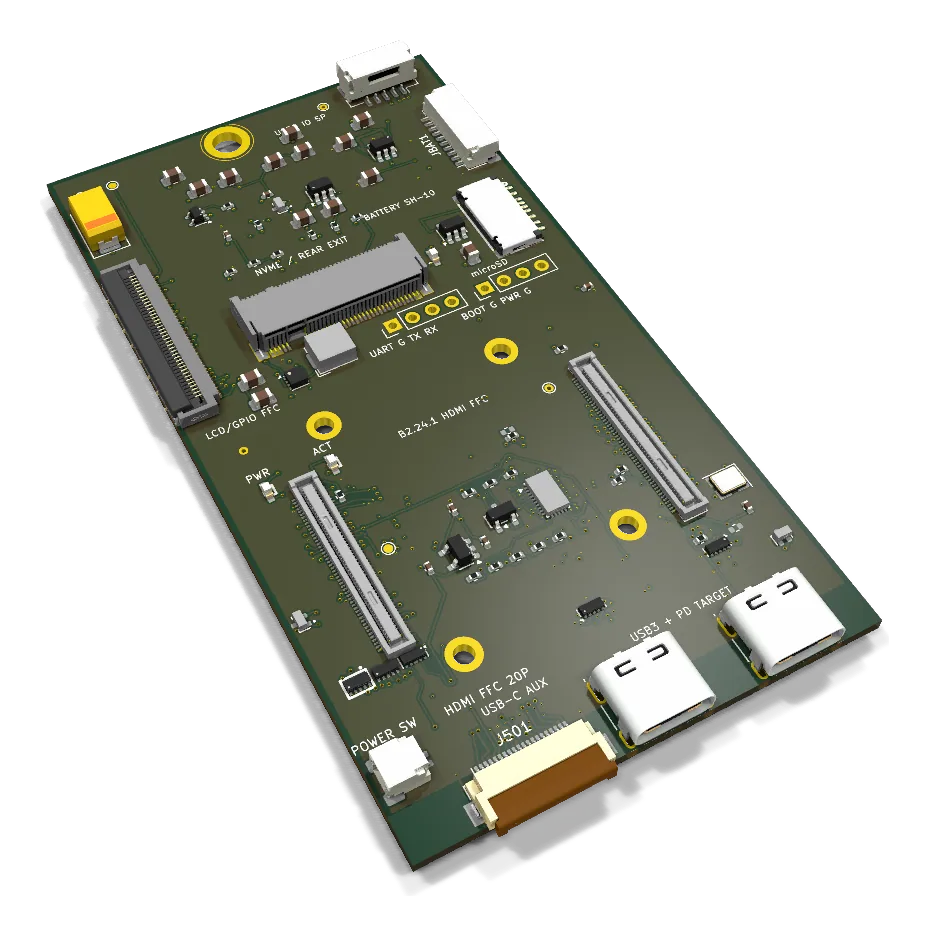
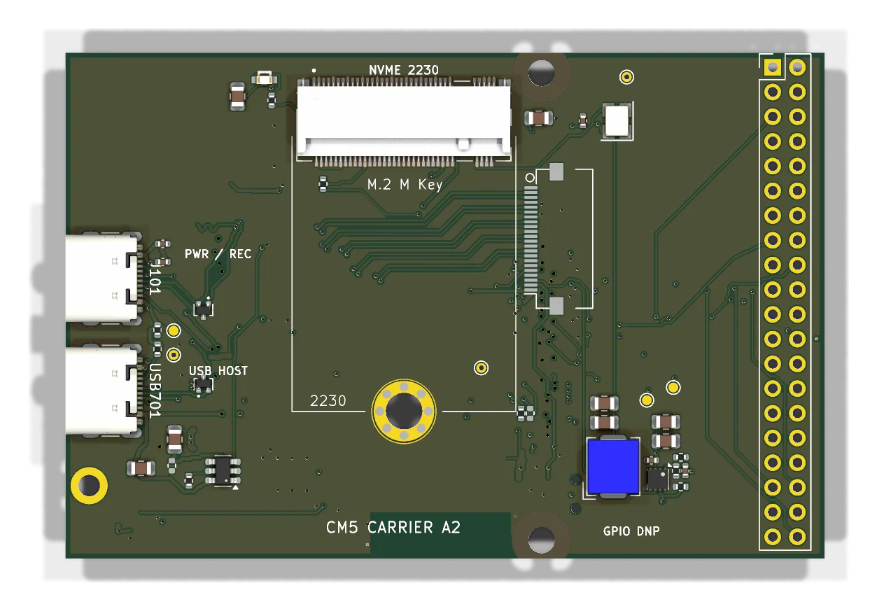
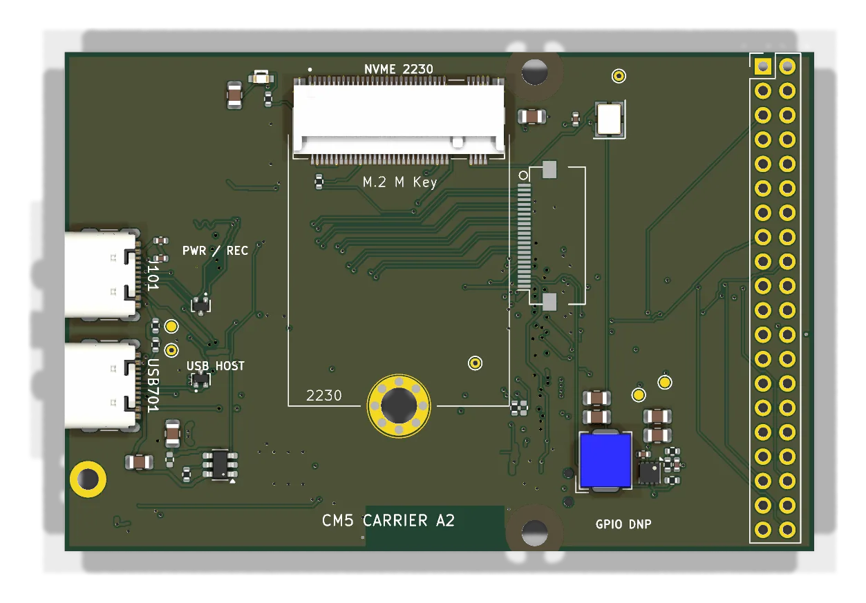
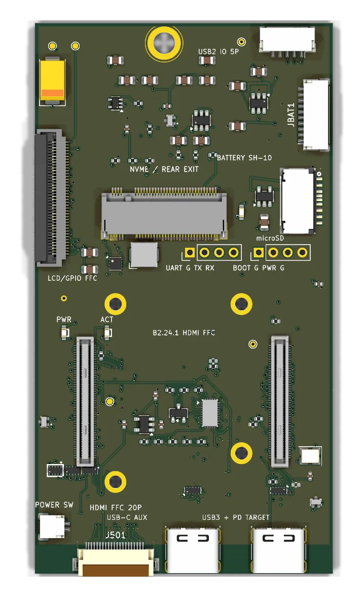
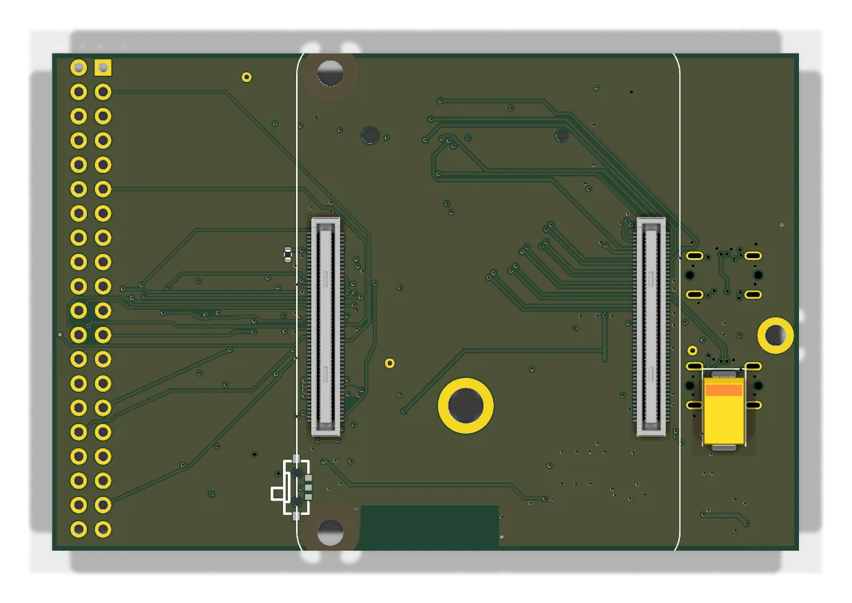
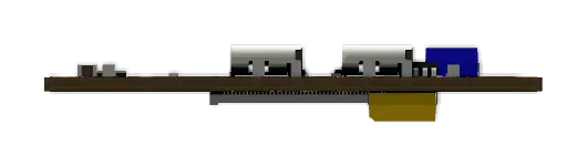
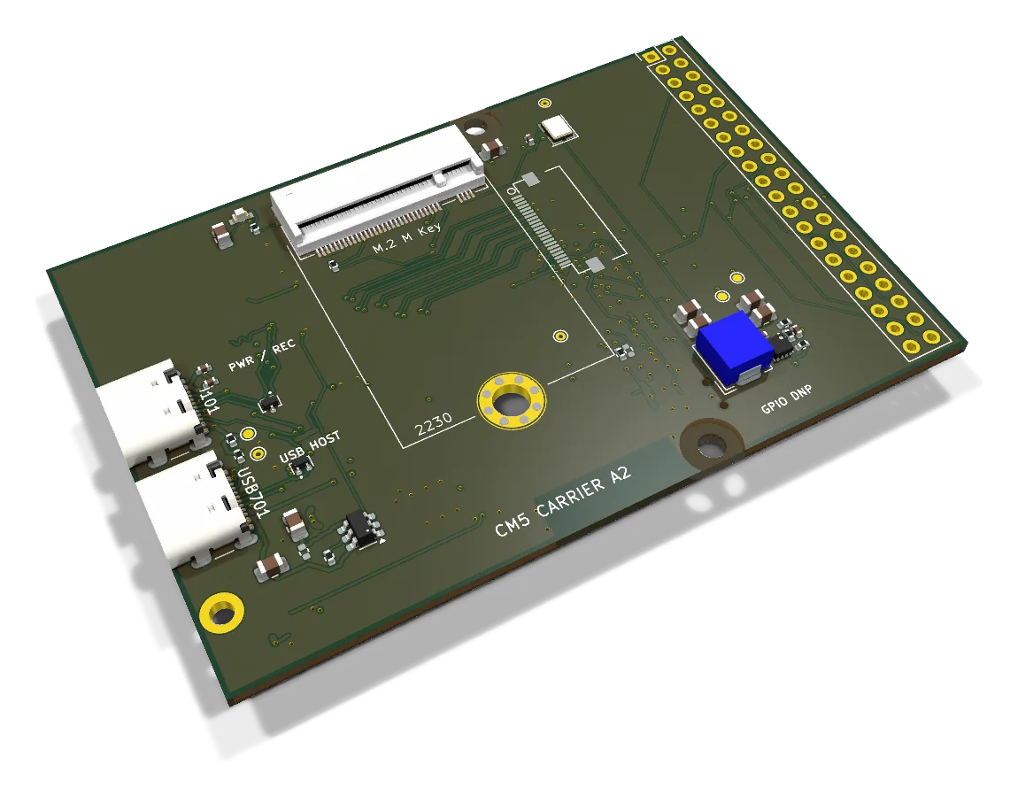
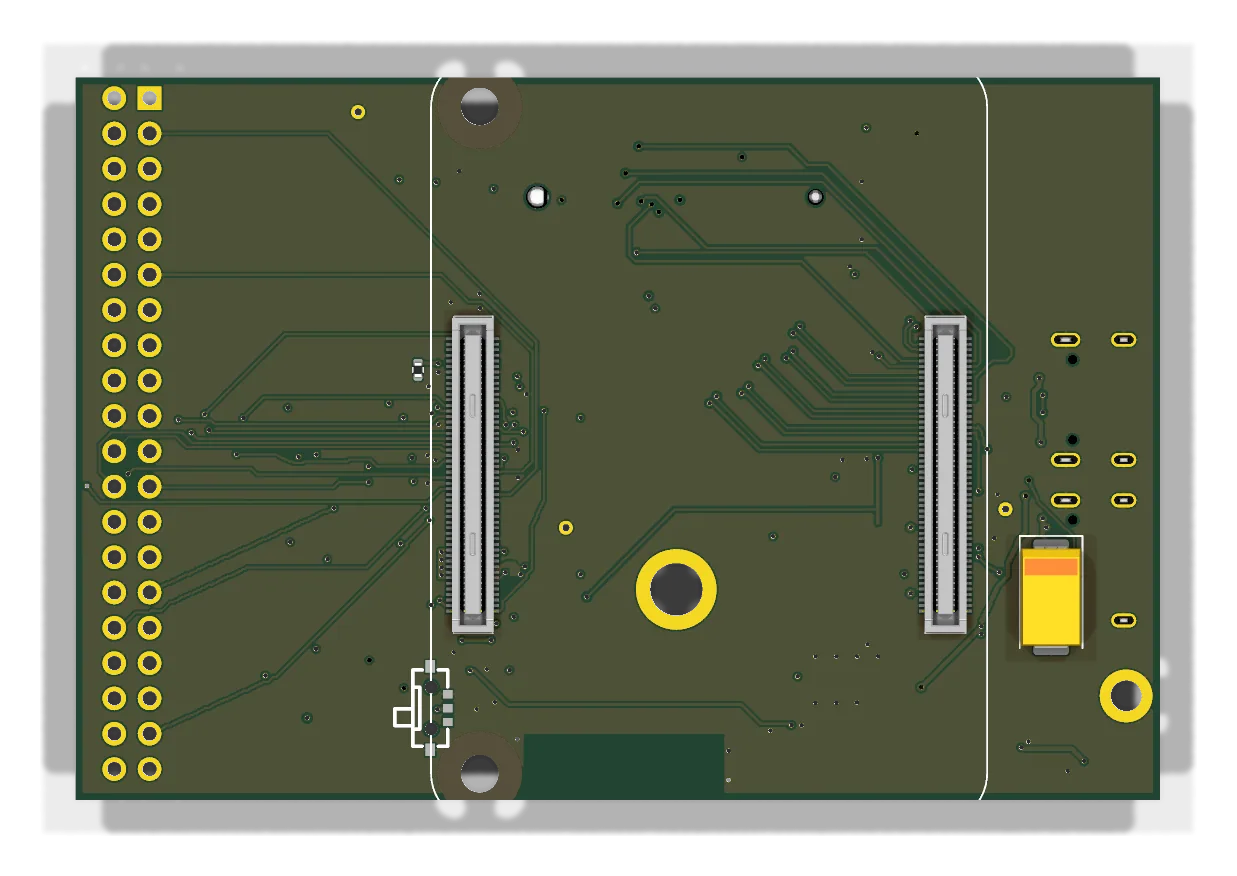
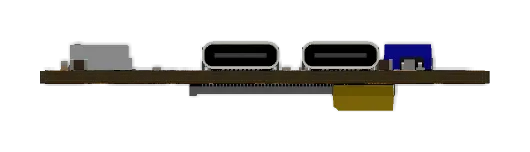
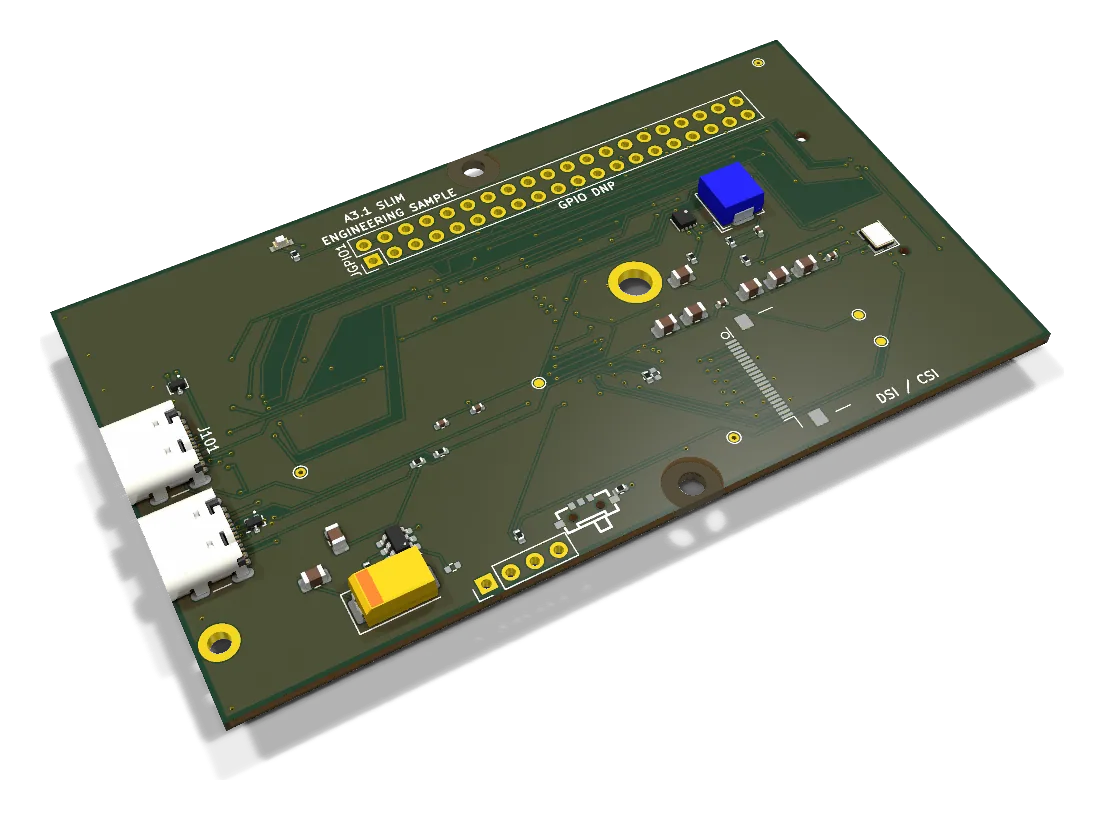
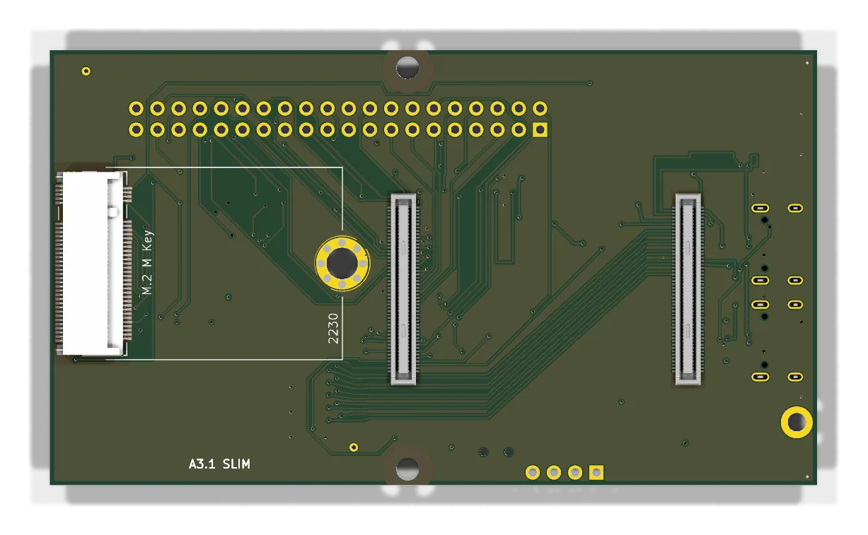
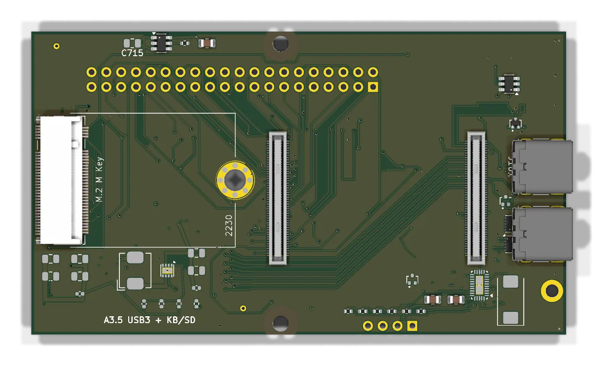
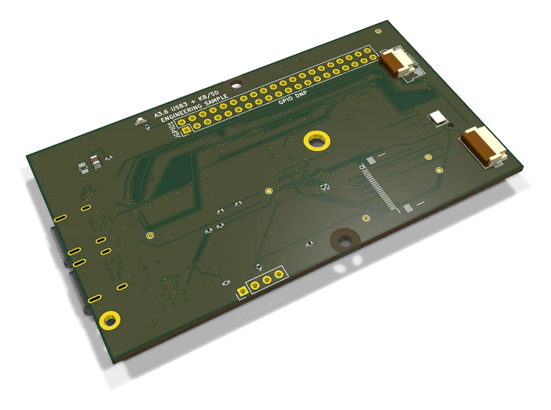
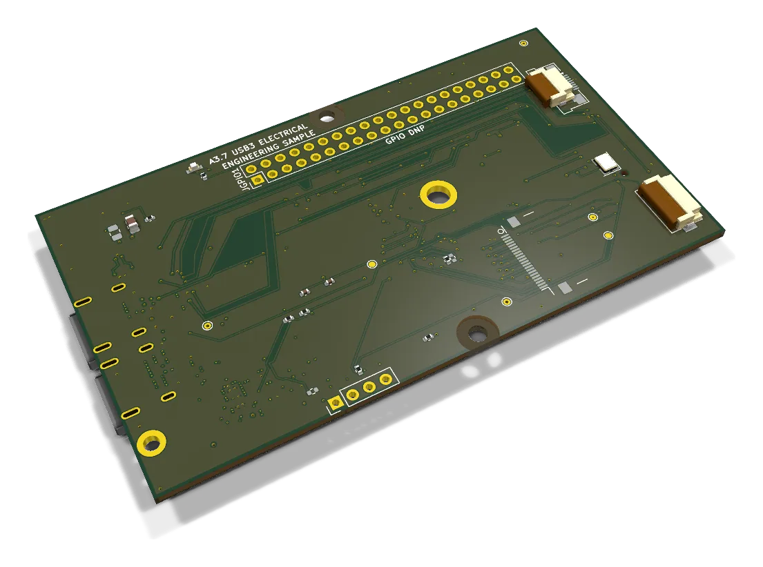
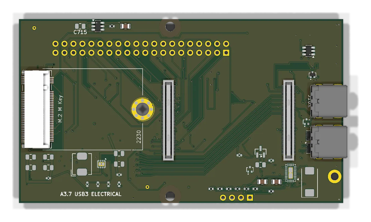
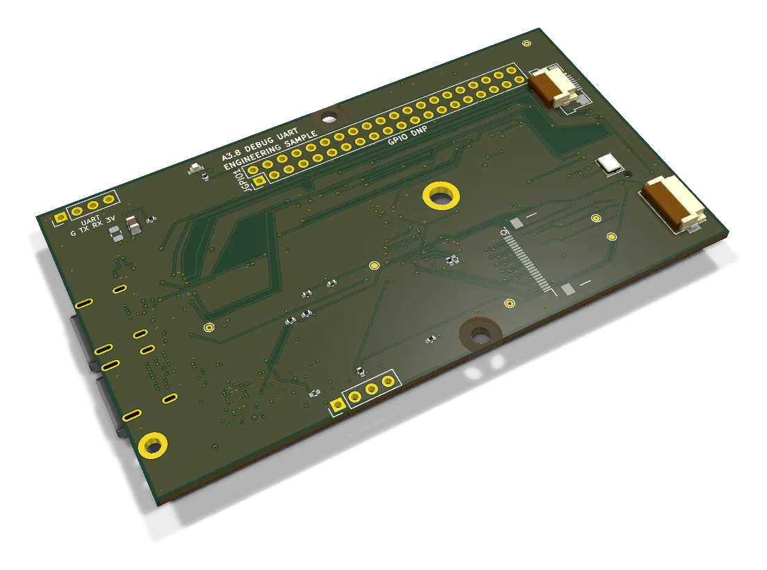
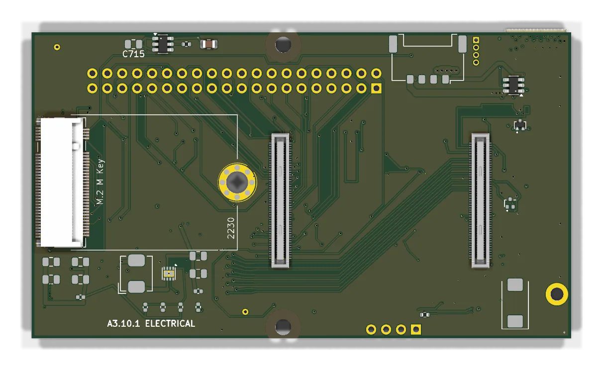
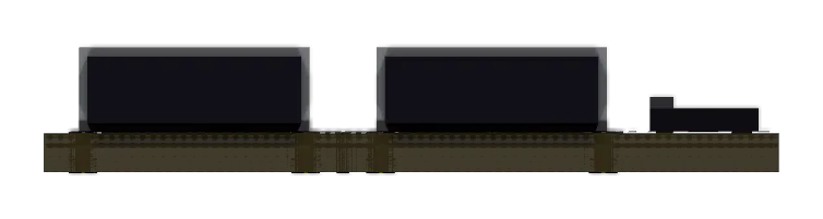
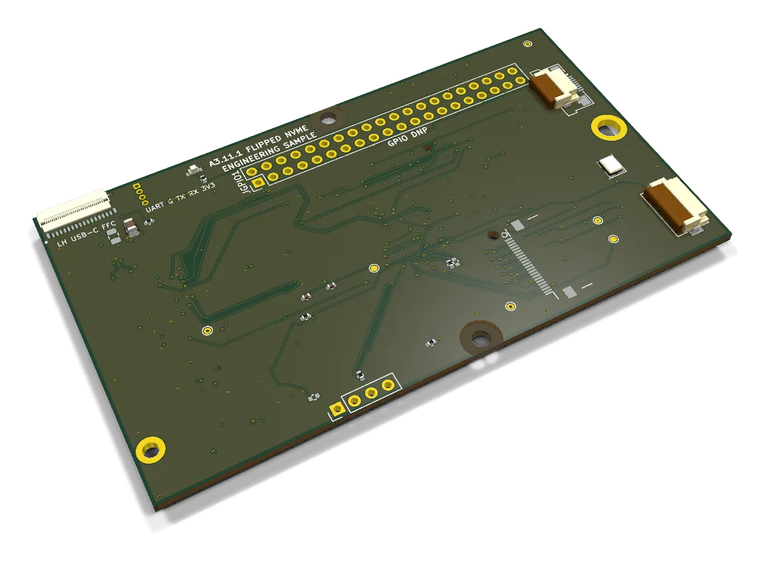
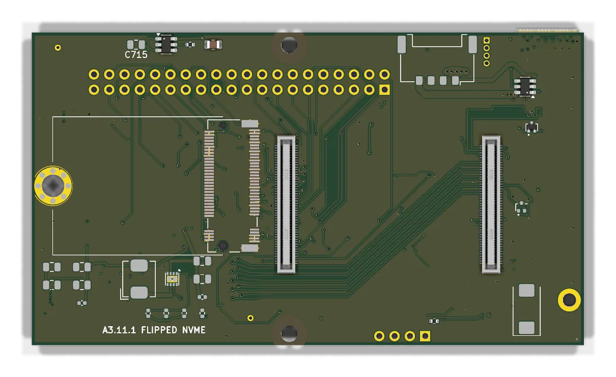
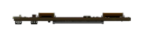
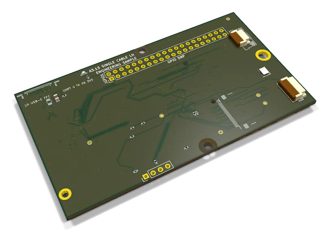
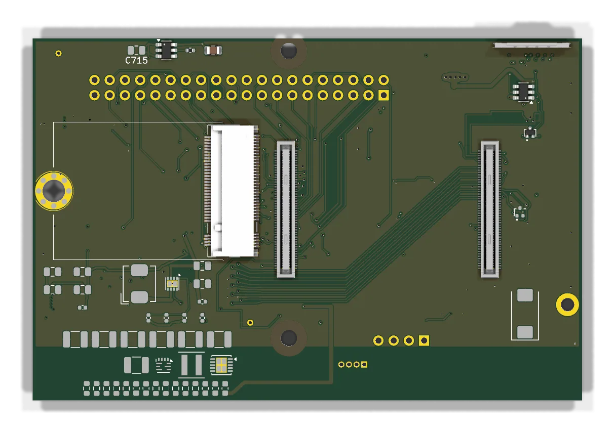
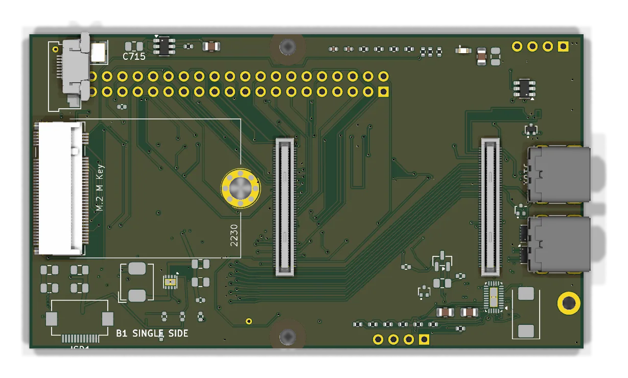
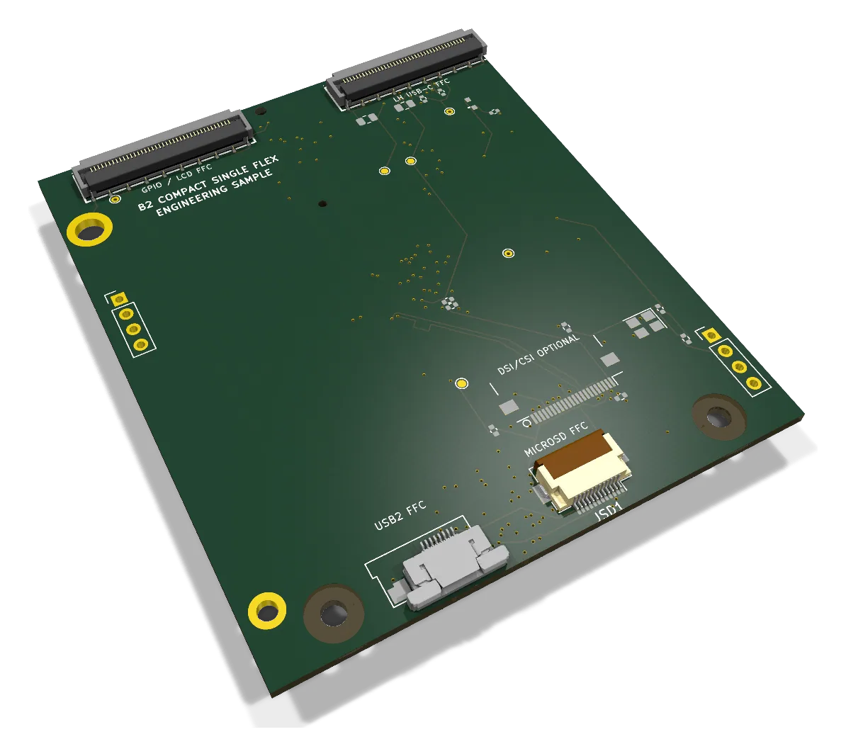
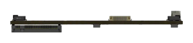
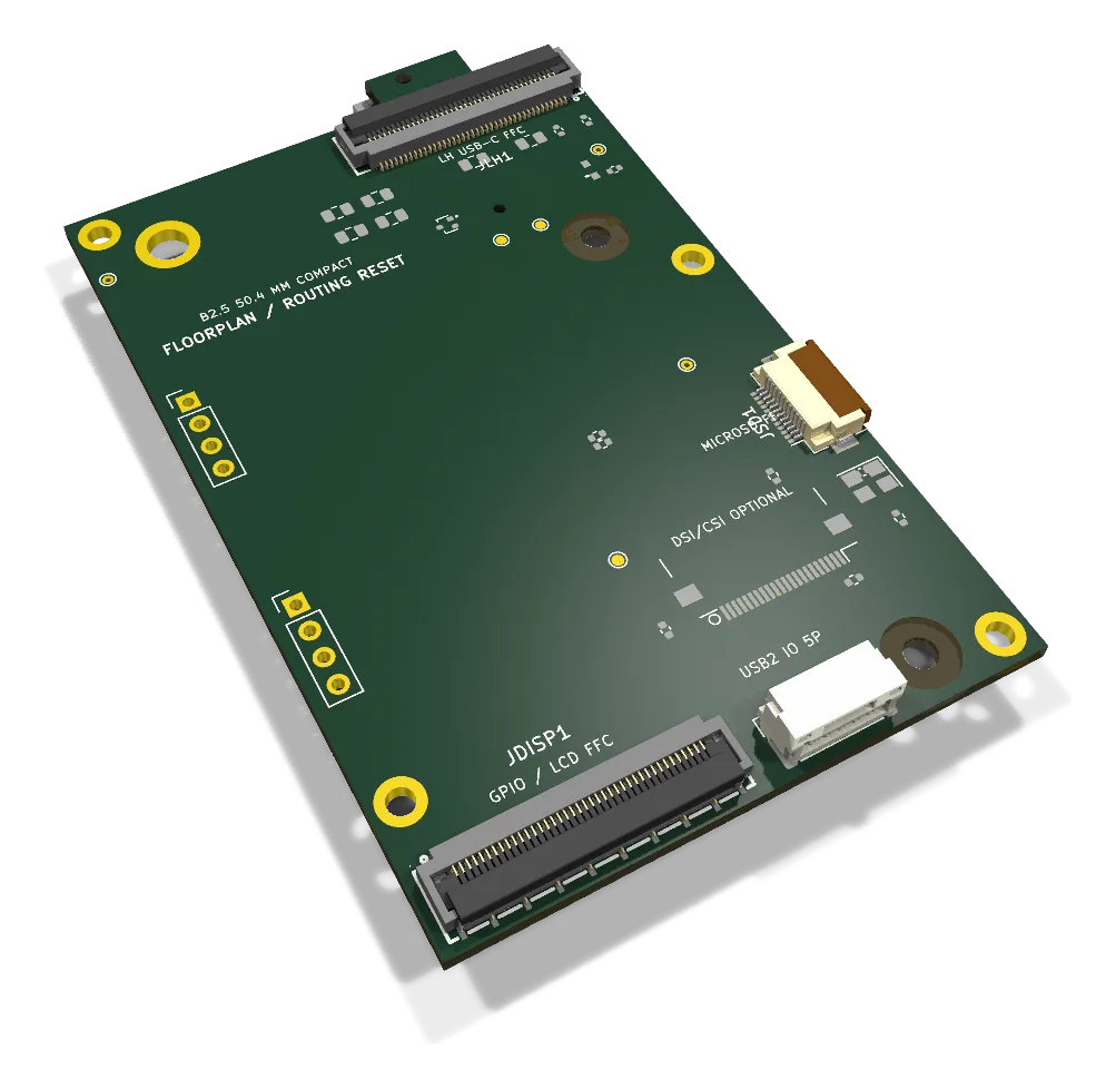
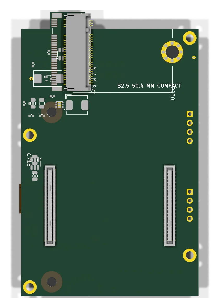
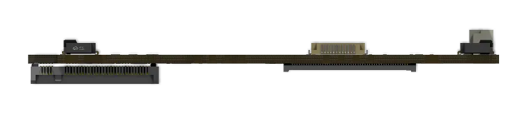
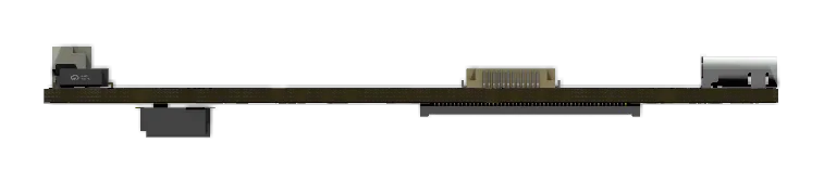
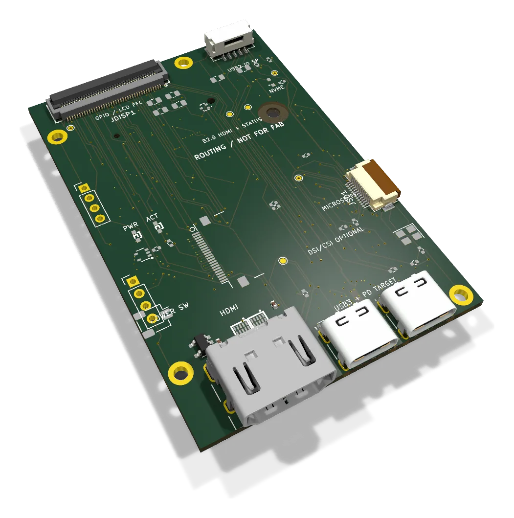
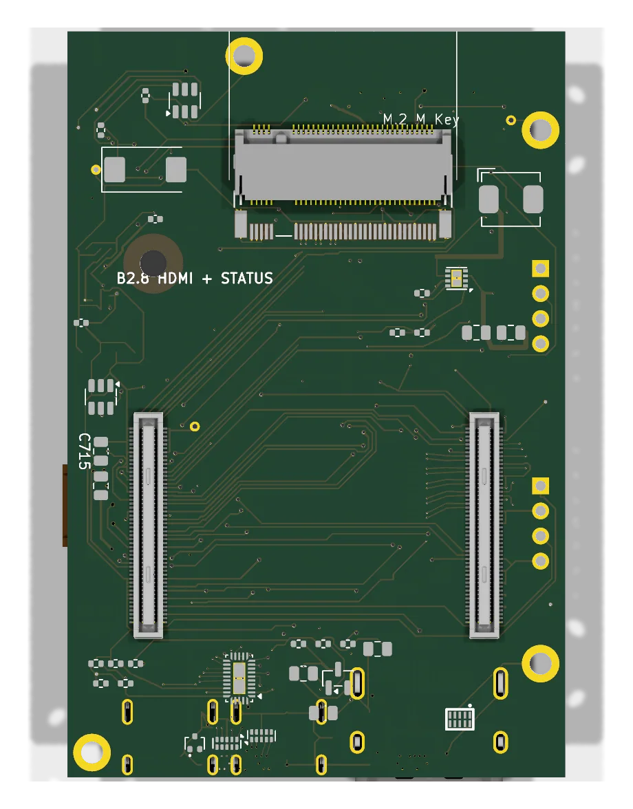
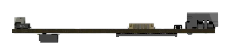
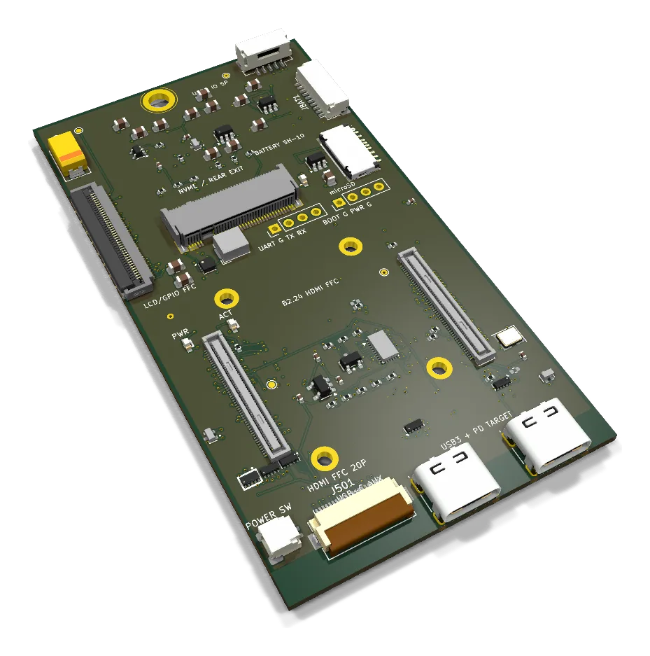
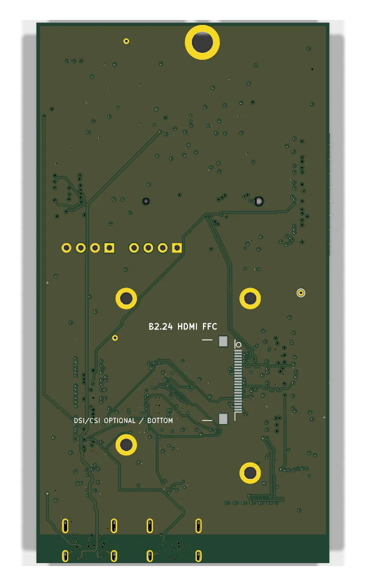
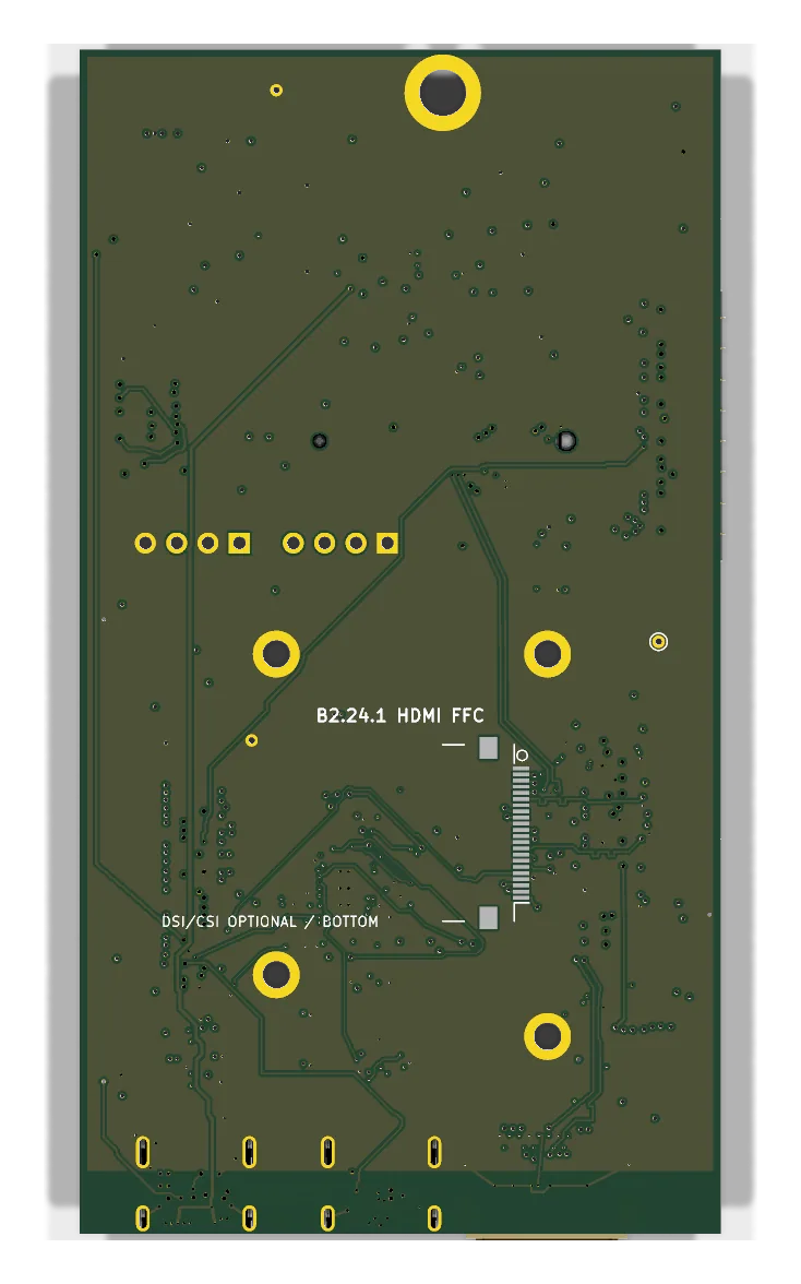
B2.24.1 Top-side 20-pin HDMI FFC
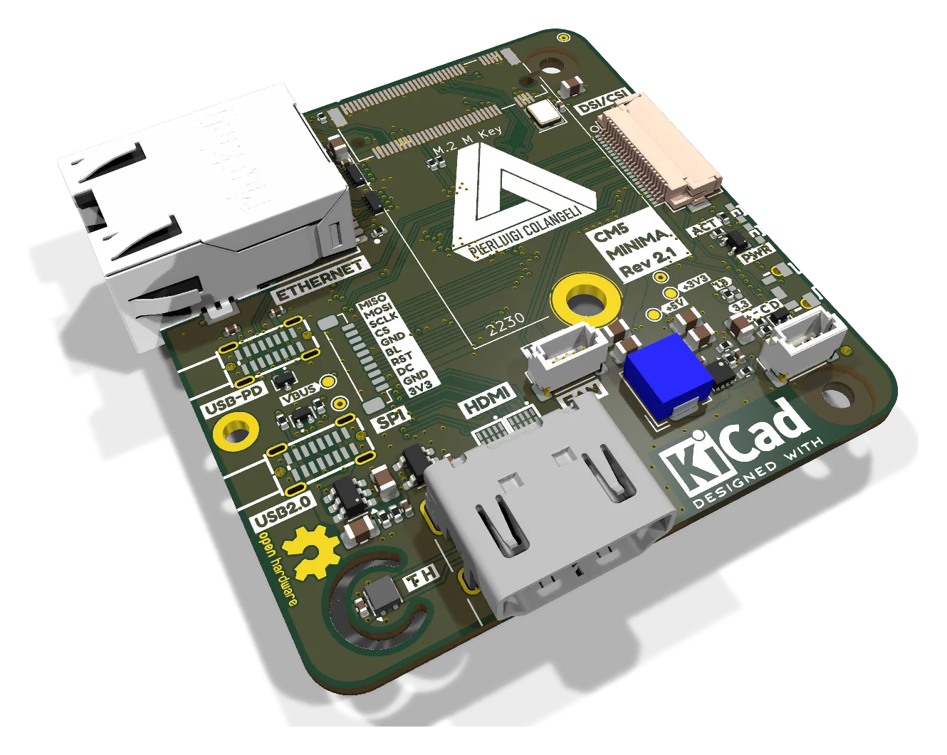
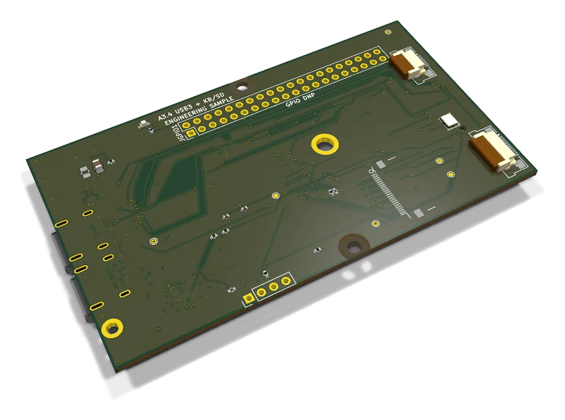
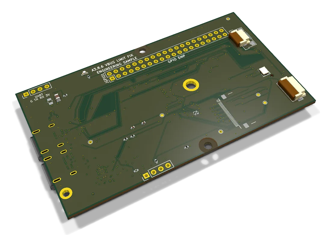
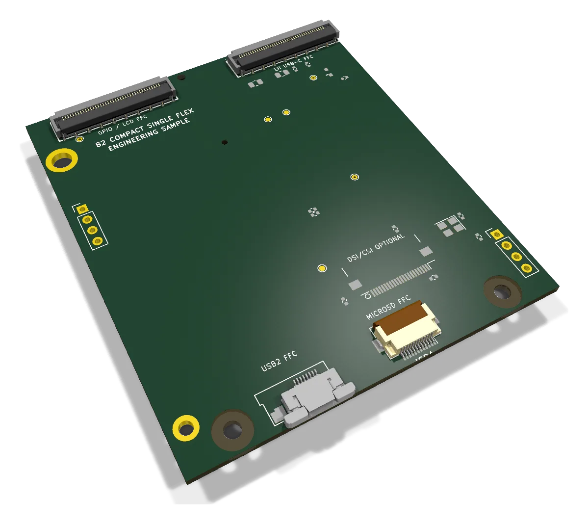
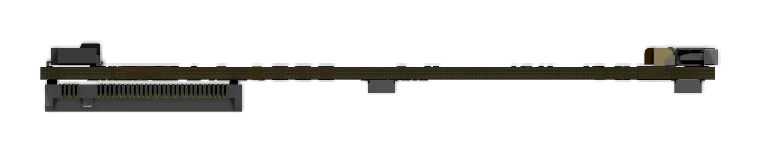
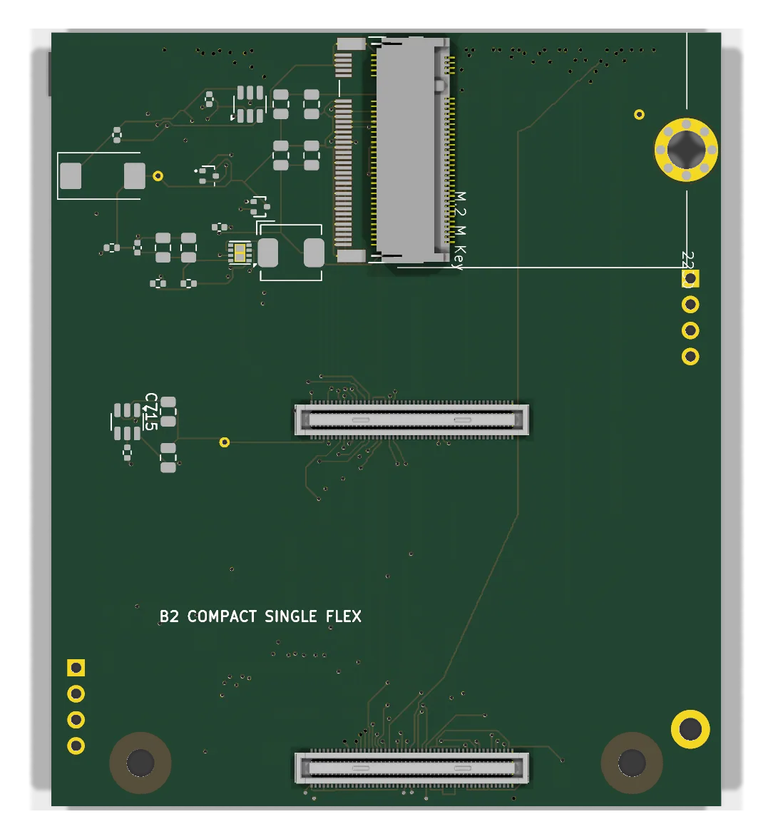
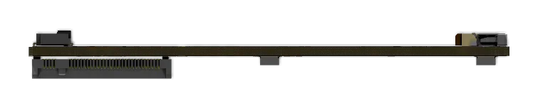
B2.24.1 perspective render
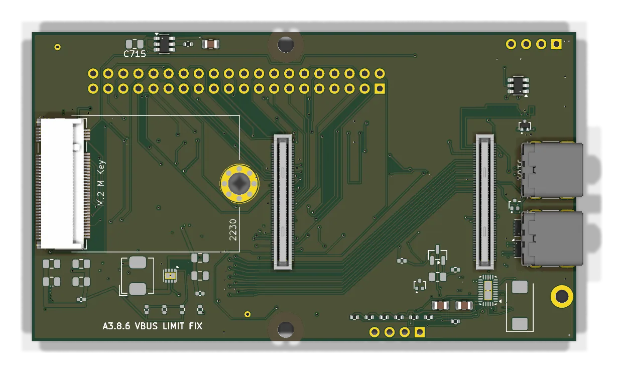
52 × 96 mm
6 COPPER LAYERS

Lineage

Where the design branched.

Left to right in date order, one lane per concurrent line. A ring marks a revision that forked more than once; a diamond marks one restarted from an earlier baseline while re-applying a later floorplan. Click a node to jump to its revision.

LH port card supersedes LH flex B2.17 restarted from B2.15.2 B2.17 floorplan re-applied B2.16 Rev 2 — CM5 MINIMA Rev 2 upstream fork (Upstream seed, 2026-07-30) Rev 2 A0 — First fabrication package (Historic, 2026-07-30) A0 A1 — Populated-envelope fit gate (Historic, 2026-07-30) A1 A2 — Released five-board prototype (Paid prototype order · placement stop, 2026-07-31) A2 A3.1 — Slim carrier (Fabrication gated, 2026-07-31) A3.1 A2.1 — Isolated correction candidate (Correction candidate, 2026-08-01) A2.1 A3.2 — Low profile (Electrically gated, 2026-08-01) A3.2 A3.3 — Right-side USB 2.0 and microSD (DRC/ERC clean, 2026-08-02) A3.3 A3.4 — Left-side USB 3 (JLC candidate, 2026-08-02) A3.4 A3.4a — Stocked microSD FFC connector (Sourcing fork, 2026-08-03) A3.4a A3.5 — Fabrication candidate (Electrical review closed, 2026-08-03) A3.5 A3.6 — Stocked Hirose microSD connector (Sourcing fork, 2026-08-03) A3.6 A3.7 — USB 3 electrical closure (USB 3 electrically closed, 2026-08-03) A3.7 A3.8 — Debug UART (Debug UART added, 2026-08-03) A3.8 LH flex — Left-hand USB-C flex daughter card (Superseded, 2026-08-03) LH flex A3.9 — Left-hand USB-C daughter card (Architecture change, 2026-08-04) A3.9 A3.10 — Top-edge FFC placement (Placement study · routing gate fails, 2026-08-04) A3.10 A3.10.1 — Electrical closure and live quote (Live quote · sockets short, 2026-08-04) A3.10.1 LH port card — Left-hand USB-C rigid port card (Companion card, 2026-08-04) LH port card A3.11.1 — Flipped NVMe closure (Head of merged A3 line, 2026-08-05) A3.11.1 A3.8.1 — JLC closure (JLC closure, 2026-08-06) A3.8.1 A3.8.2 — JLC BOM closure (JLC BOM closure, 2026-08-06) A3.8.2 A3.8.3 — Stocked QCHT USB-C evaluation (Connector evaluation, 2026-08-06) A3.8.3 A3.13 — Single-cable left-hand carrier (Unmerged work in progress, 2026-08-06) A3.13 A3.14 — Cost-reduced single-cable carrier (Unmerged work in progress, 2026-08-06) A3.14 A3.8.4 — QCHT-native routing closure (Rejected connector study, 2026-08-07) A3.8.4 A3.8.5 — JLC upload snapshot (Uploaded for quote, 2026-08-07) A3.8.5 A3.8.6 — VBUS current-limit correction (Electrical correction, 2026-08-07) A3.8.6 A3.8.7 — Connector and fabrication correction — the fabricated board (Fabricated · 5 boards received, 2026-08-07) A3.8.7 B1 — Single-sided assembly prototype (Assembly prototype, 2026-08-07) B1 B2.0 — Compact single-FFC architecture fork (Architecture fork · unrouted, 2026-08-09) B2.0 B2.1 — Routed single-FFC carrier (Routed, 2026-08-10) B2.1 B2.2 — LCD interface production revision (LCD interconnect revision, 2026-08-13) B2.2 B2.3 — Matching USB interconnect (Interconnect contract match, 2026-08-14) B2.3 B2.4 — Bottom-edge connectors (Routing checkpoint, 2026-08-15) B2.4 B2.5 — Rotated CM5, 15 mm narrower (Compact floorplan, 2026-08-15) B2.5 B2.6 — Dual direct USB-C, left NVMe (Mechanical floorplan checkpoint, 2026-08-15) B2.6 B2.7 — Direct USB-C fabrication routing (Fab gated · 6 opens, 2026-08-16) B2.7 B2.9 — Protected-2S battery interface (Interface checkpoint, 2026-08-17) B2.9 B2.8 — HDMI, status LEDs and power switch (Fabrication blocked, 2026-08-19) B2.8 B2.11 — Top-side CM5 and Mini HDMI (Work in progress, 2026-08-19) B2.11 B2.12 — Rotated CM5, edge I/O (Placement reset, 2026-08-19) B2.12 B2.13 — CM5 right, SD I/O restored (Placement reset, 2026-08-19) B2.13 B2.14 — Bottom height reduction (Height reduction, 2026-08-19) B2.14 B2.14.1 — Fabrication routing checkpoint (Routing checkpoint, 2026-08-19) B2.14.1 B2.14.2 — Routing and height review (Routing checkpoint, 2026-08-20) B2.14.2 B2.15 — Flush bottom, onboard 2230 (Mechanical decision · unrouted, 2026-08-20) B2.15 B2.15.1 — Native reroute (Fabrication-ready routing, 2026-08-21) B2.15.1 B2.15.2 — Complete 3D model coverage (DRC clean baseline, 2026-08-21) B2.15.2 B2.15.3 — CM5 clearance floorplan (Routing checkpoint · opens, 2026-08-21) B2.15.3 B2.15.4 — microSD and top-edge USB 2.0 (Routed prototype, 2026-08-21) B2.15.4 B2.16 — JST PH-8 battery link (Electrically invalid, 2026-08-22) B2.16 B2.17 — Native fabrication-routing restart (Native routing checkpoint, 2026-08-22) B2.17 B2.17.1 — microSD top-edge USB 2.0 candidate (Candidate, 2026-08-22) B2.17.1 B2.17.2 — Service silkscreen (Silkscreen only, 2026-08-22) B2.17.2 B2.18 — GH-10 battery-link prototype (Battery-link prototype, 2026-08-22) B2.18 B2.19 — SH-10 battery link (Released and quoted, 2026-08-23) B2.19 B2.20 — 1.5 mm CM5 socket clearance (Electrically closed · quoted, 2026-08-23) B2.20 B2.21 — CM5 assembly-rotation correction (Placement fix · vias rejected, 2026-08-24) B2.21 B2.22 — Through-via correction (Released, 2026-08-24) B2.22 B2.23 — USB 3 RX2 skew correction (Withdrawn · mirrored footprints, 2026-08-24) B2.23 B2.24 (tscircuit) — tscircuit DSI/CSI placement experiment (Routing experiment, 2026-08-26) B2.24 (tscircuit) B2.24 (charger) — Charger and NVDC design start (Design start · not fab-ready, 2026-08-29) B2.24 (charger) B2.23.1 — Mirrored-footprint correction (Gates pass · candidate, 2026-08-31) B2.23.1 B2.23.2 — Manufacturing-minima correction (Uploaded for review, 2026-08-31) B2.23.2 B2.23.3 — RX1 skew tuning (Head of main, 2026-08-31) B2.23.3 B2.24 — 20-pin HDMI FFC fork (Development fork, 2026-09-01) B2.24 B2.24.1 — Top-side 20-pin HDMI FFC (Fabrication release · latest, 2026-09-02) B2.24.1

67 revisions carry a compressed glTF model. With this many, each loads on request; up to six stay live at once.

Contact sheet

68 boards at a glance.

Every revision in lineage order, left to right and wrapping. A tile that does not continue from the one before it shows where it forked from. True scale sizes each board by its real outline, so you can watch the carrier grow, shrink and turn.

Revisions

One board, 68 physical decisions.

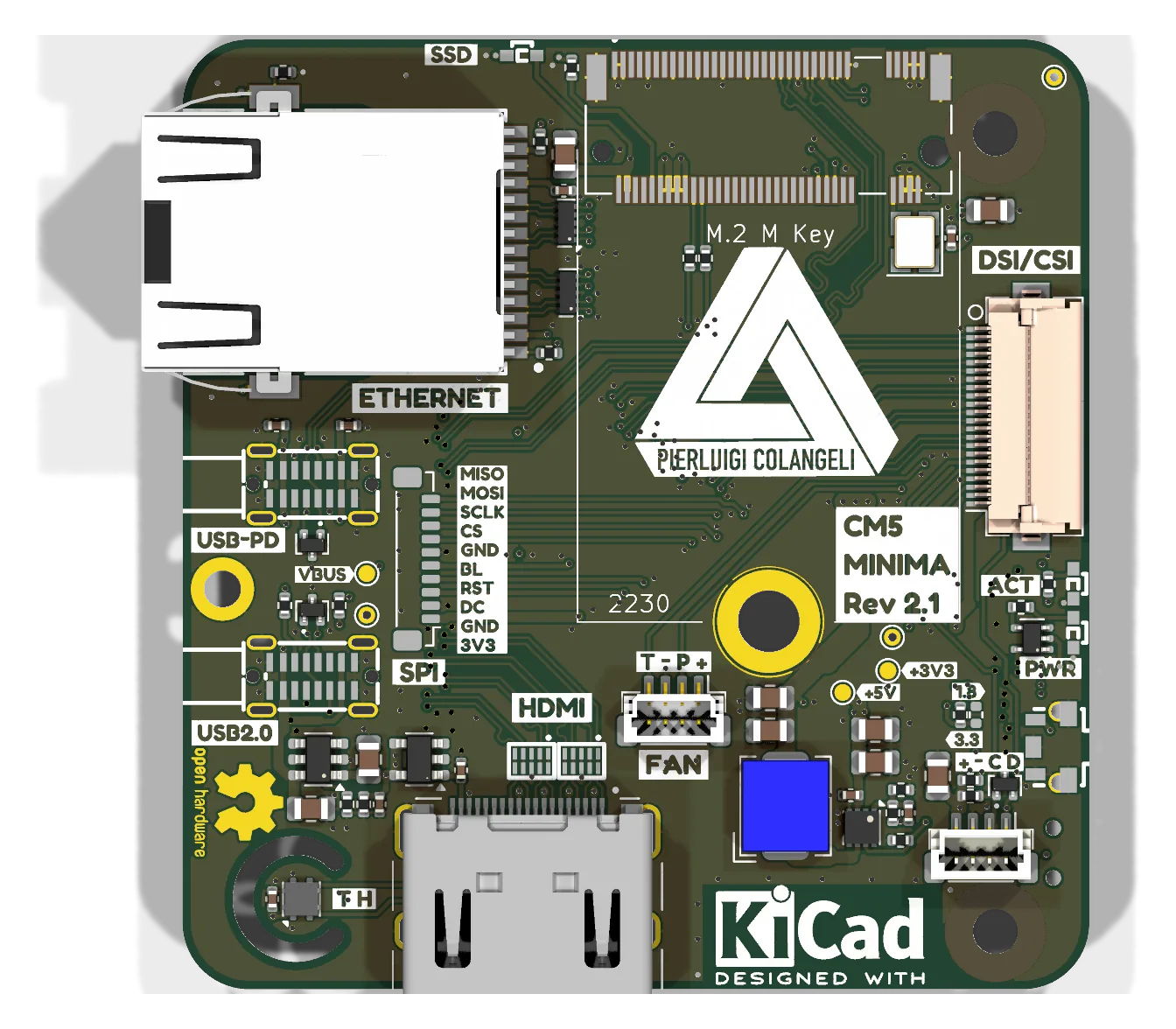
Rev 2

CM5 MINIMA Rev 2 upstream fork

Upstream seed Upstream seed upstreamMINIMA

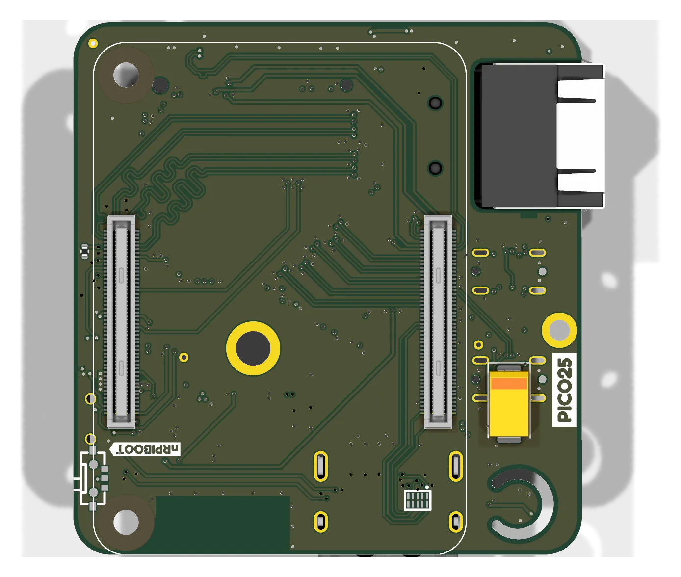
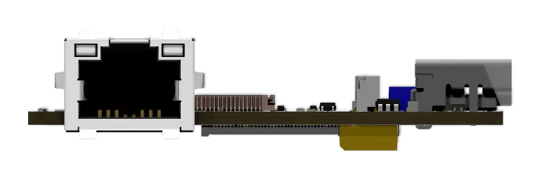
The untouched open-source seed: the smallest routed, manufactured CM5 carrier with same-edge USB-C ports and onboard M.2 2230 NVMe. Kept in the tree so every later change can be diffed against its source.

Outline
54.55 × 57.14 mm
Layers
6 Cu
Footprints
102
Branch
main
Commit
53aadf4
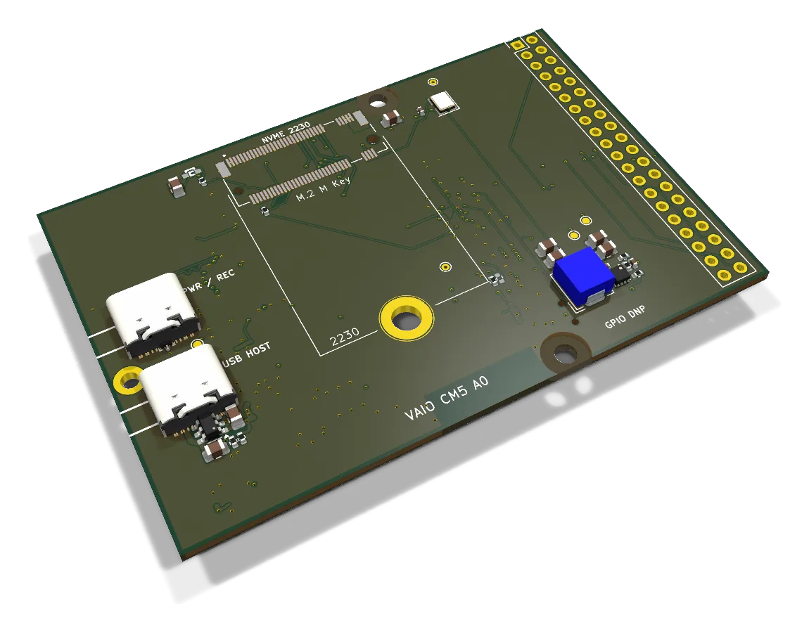
Rev 2 perspective render

Continues as A0

Notes Open-source base review
A0

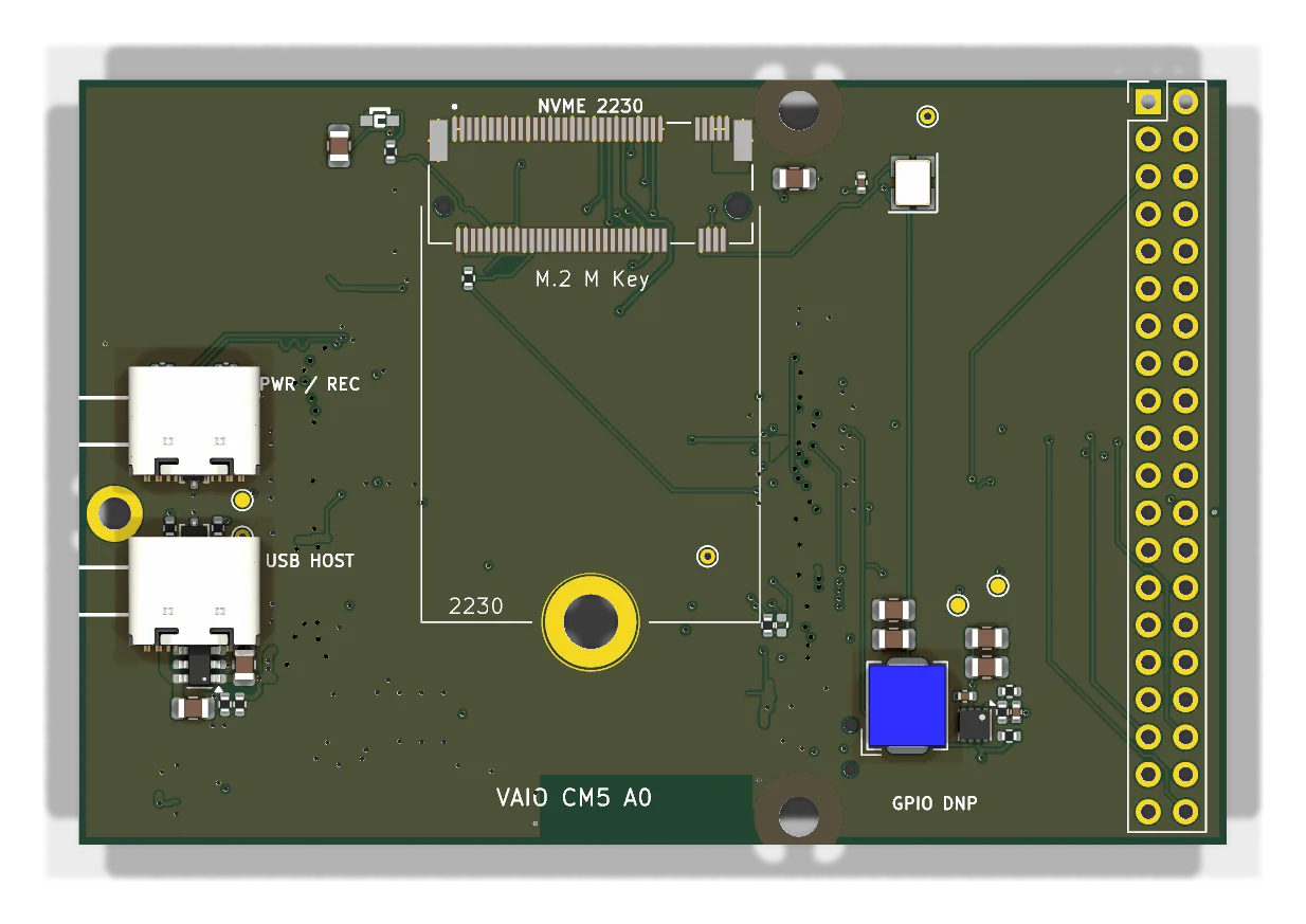
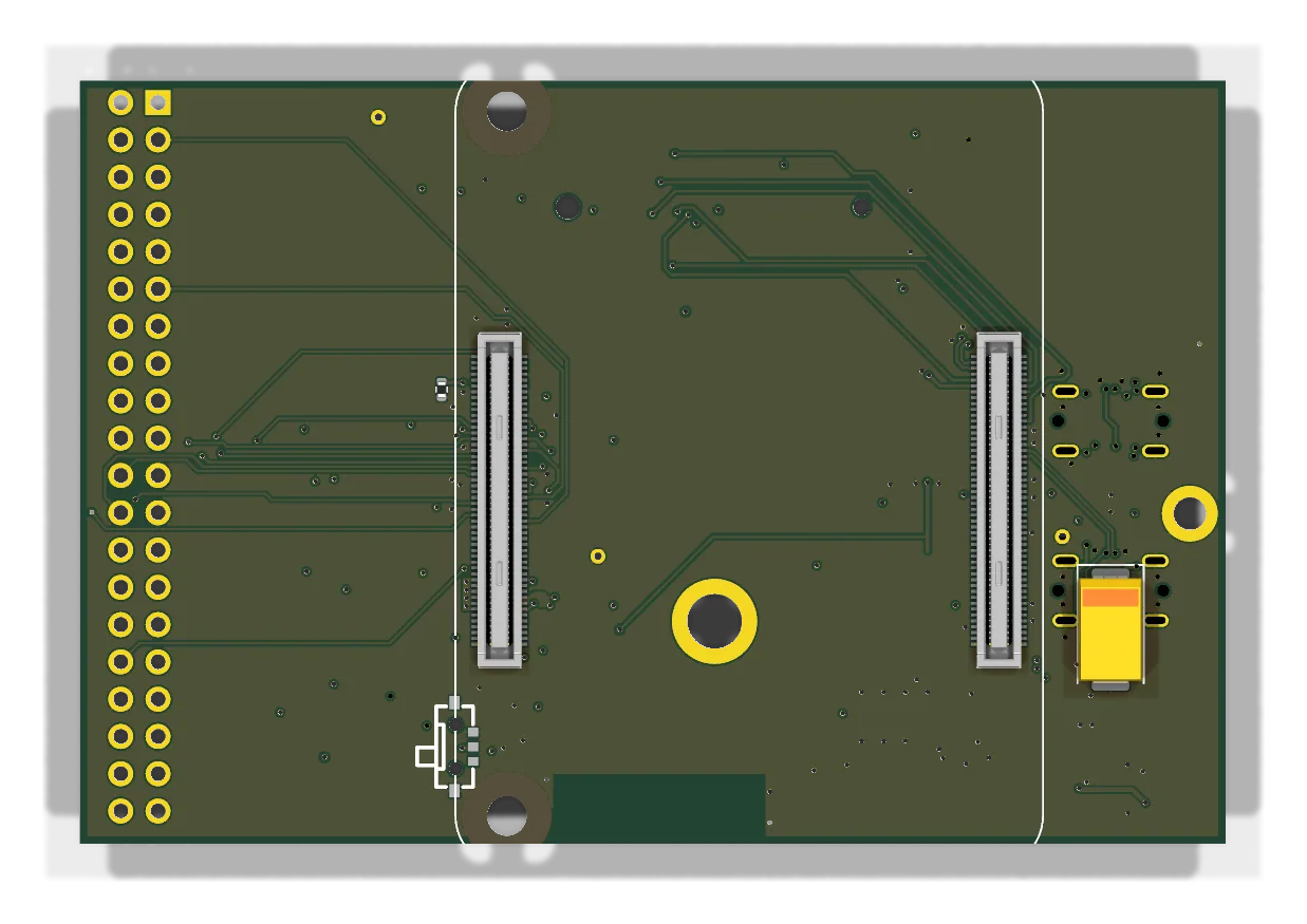
First fabrication package

Historic A line · 78 × 52 mm

First fabrication package cut from the MINIMA fork. Establishes the 78 × 52 mm outline and the six-layer stack that A1 and A2 inherit.

Outline
78 × 52 mm
Layers
6 Cu
Footprints
48
Branch
main
Commit
b53eba5242
A0 perspective render
A1

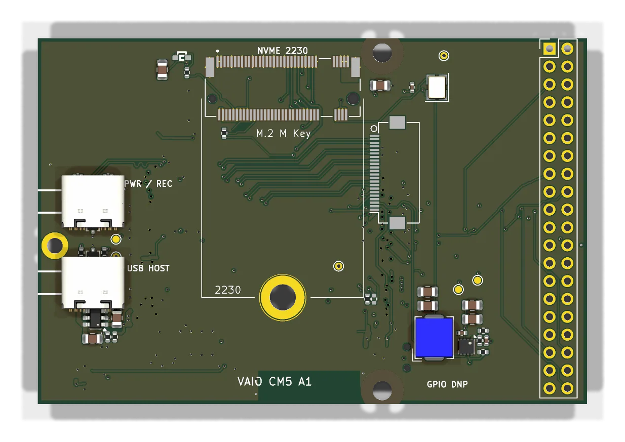
Populated-envelope fit gate

Historic A line · 78 × 52 mm

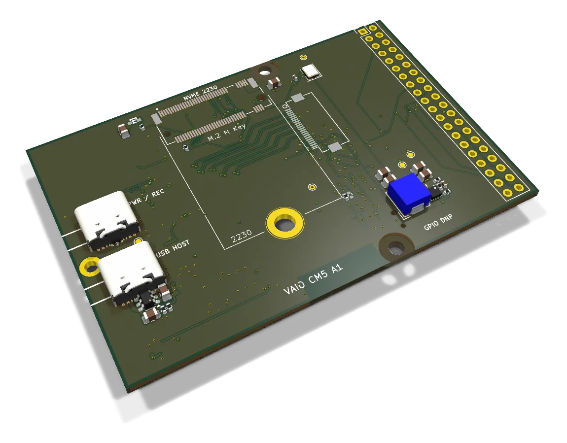
Adds the populated-envelope fit gate that every later revision is measured against. Outline and stackup unchanged.

Outline
78 × 52 mm
Layers
6 Cu
Footprints
49
Branch
main
Commit
5a7b8705d9
A1 perspective render

From A0

Continues as A2

Notes Incremental bring-up
A2

Released five-board prototype

Paid prototype order · placement stop A line · 78 × 52 mm ordered

The released prototype with corrected USB-C orientation and stocked assembly connectors. CM5 sockets sit on the back opposite the SSD, which drives the 9.77 mm populated envelope, the tallest of any revision. The order carries a documented stop on the submitted placement file.

Outline
78 × 52 mm
Layers
6 Cu
Footprints
49
Envelope
9.77 mm populated
Branch
main
Commit
a976693
A2 perspective render

From A1

Continues as A2.1 A3.1

Notes Independent A2 reviewJLCPCB order handoffSubmitted placement stop
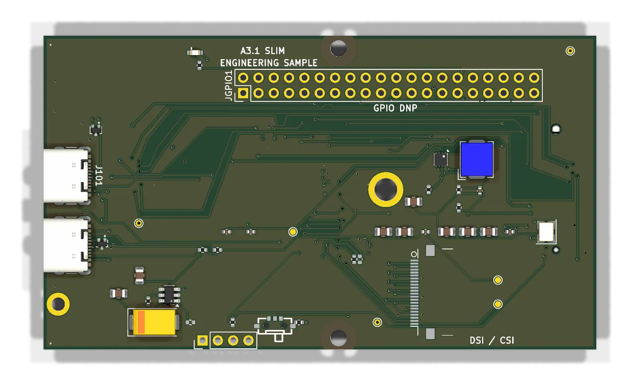
A3.1

Slim carrier

Fabrication gated A3 line · 91.69 × 52 mm

The outline grows to 91.69 × 52 mm so the CM5 and the 2230 SSD sit adjacent on the bottom face instead of opposing each other. Global height barely moves because the gain is local, not global. Fabrication gated on fine-via acceptance and on the chassis cavity being measured.

Outline
91.69 × 52 mm
Layers
6 Cu
Footprints
50
Envelope
9.65 mm populated
Branch
main
Commit
ee77116
A3.1 perspective render

From A2

Continues as A3.2

Notes A3.1 slim handoff
A2.1

Isolated correction candidate

Correction candidate A line · 78 × 52 mm

Correction fork kept in its own directory so the paid A2 design stays untouched. Same outline, stack and footprint count as A2.

Outline
78 × 52 mm
Layers
6 Cu
Footprints
49
Envelope
9.77 mm populated
Branch
main
Commit
7491b3a
A2.1 perspective render

From A2

Notes A2.1 correction status
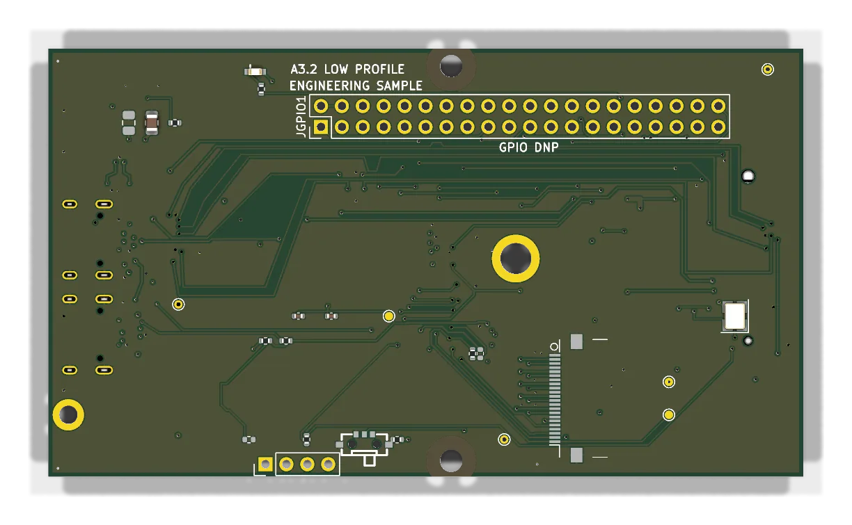
A3.2

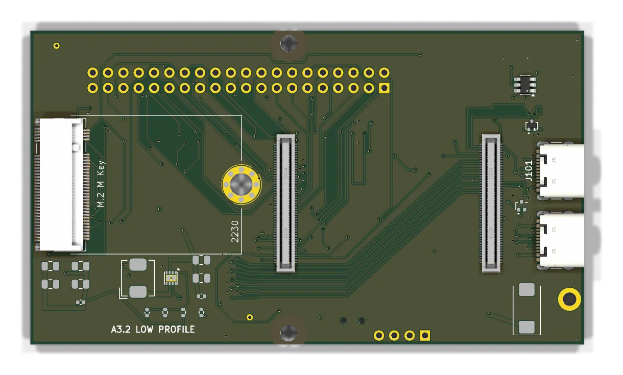
Low profile

Electrically gated A3 line · 91.69 × 52 mm

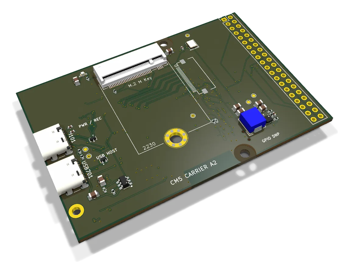
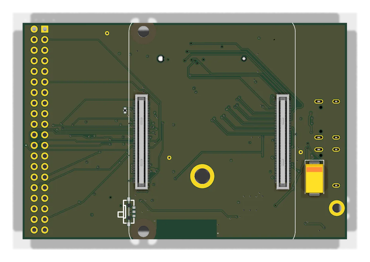
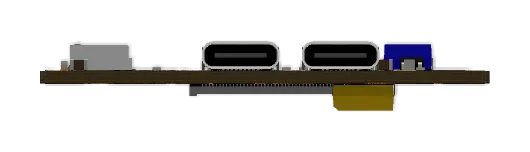
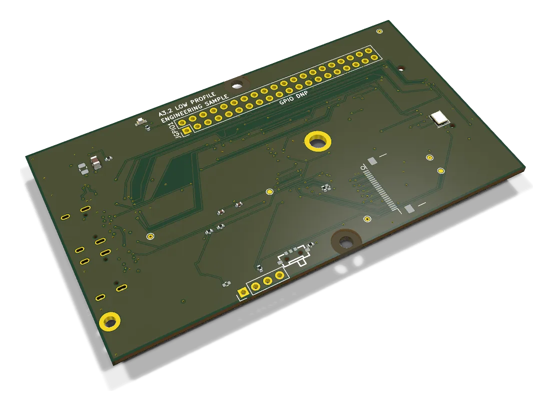
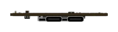
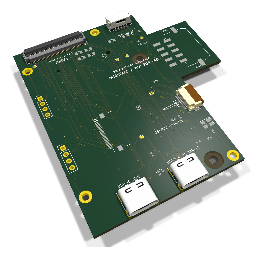
The big height win: 7.42 mm populated, 2.36 mm below A2. Both USB-C receptacles, the M.2 3.3 V regulator island and the bulk capacitor move to the back, leaving only 0.95 mm of top-side parts. The full DSI/CSI circuit stays as an optional unpopulated footprint.

Outline
91.69 × 52 mm
Layers
6 Cu
Footprints
50
Envelope
7.42 mm populated
Branch
main
Commit
0cbed0b
A3.2 perspective render

From A3.1

Continues as A3.3

Notes A3.2 low-profile handoffRelease readiness
A3.3

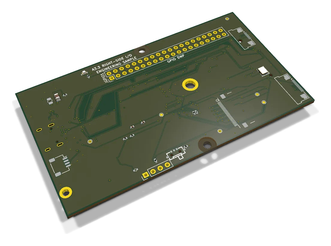
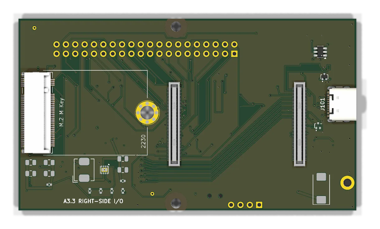
Right-side USB 2.0 and microSD

DRC/ERC clean A3 line · 91.69 × 52 mm

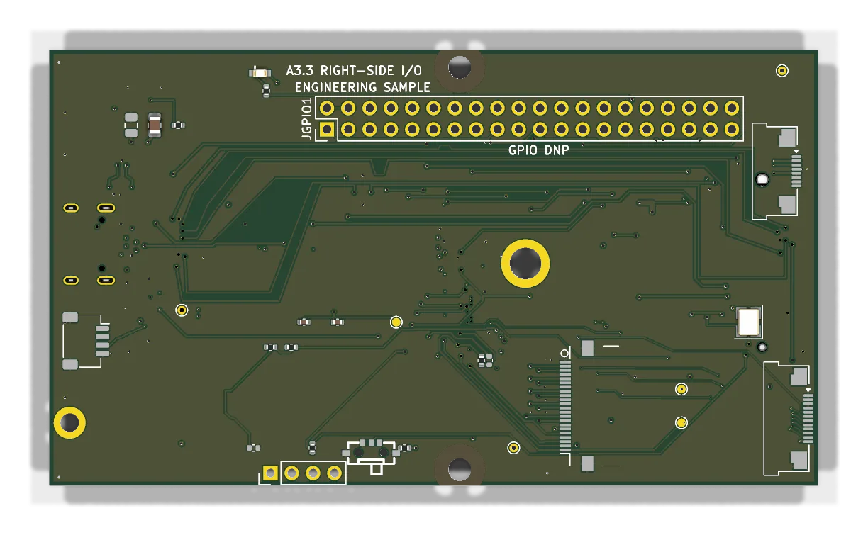
Incremental fork of A3.2 adding USB 2.0 and microSD on optional horizontal FFC landings at the right edge. Because the new I/O is unpopulated by default, the populated height stays at A3.2's figure.

Outline
91.69 × 52 mm
Layers
6 Cu
Footprints
52
Envelope
7.42 mm populated
Branch
main
Commit
f0fb284
A3.3 perspective render

From A3.2

Continues as A3.4

Notes A3.3 right-side I/O handoff
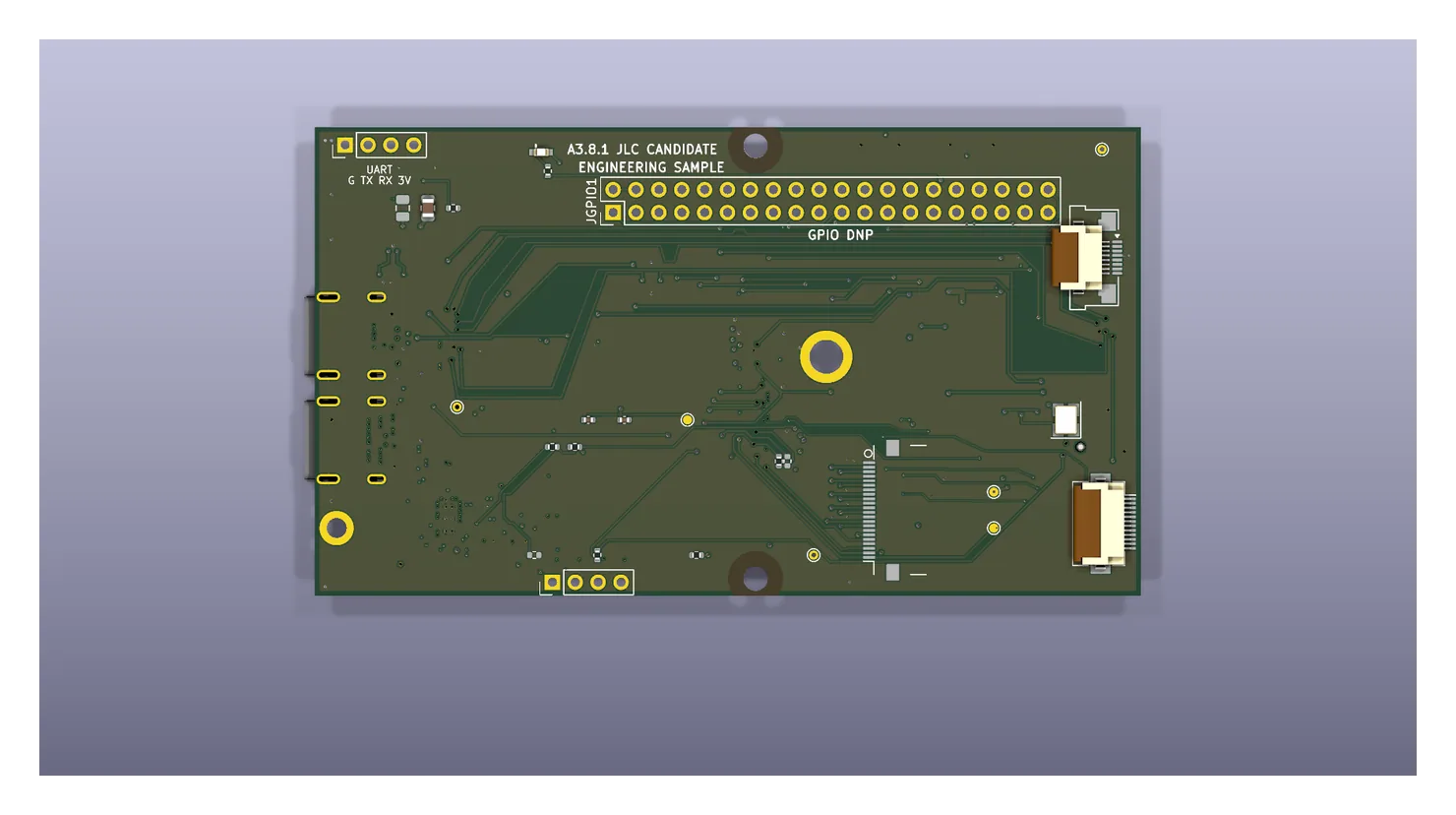
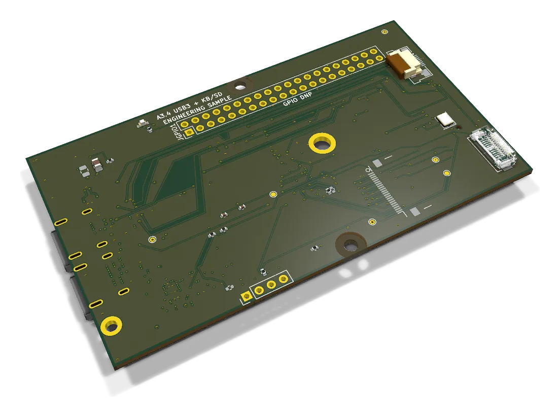
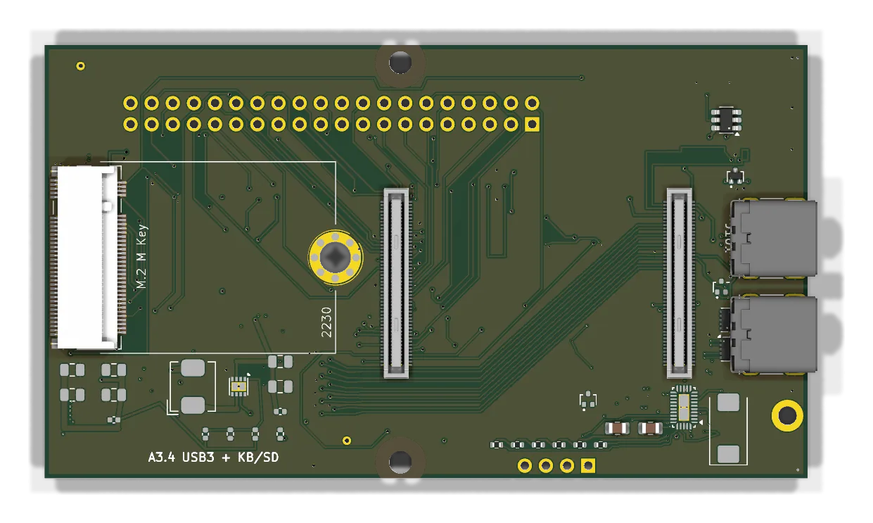
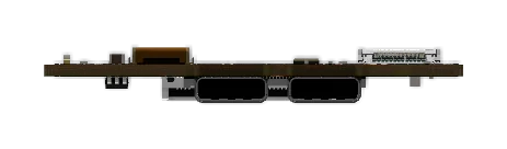
A3.4

Left-side USB 3

JLC candidate A3 line · 91.69 × 52 mm

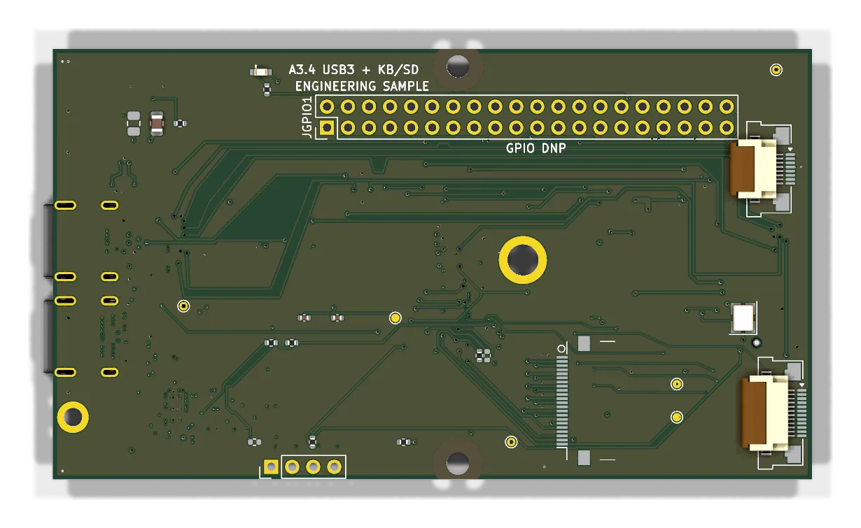
Corrects the USB role assignment: the right-side cable is the internal keyboard link and only needs USB 2.0, so USB 3 moves to the left, user-facing edge. Both Type-C positions standardise on one Molex receptacle with a TI HD3SS3220 as CC controller and SuperSpeed mux.

Outline
91.69 × 52 mm
Layers
6 Cu
Footprints
63
Branch
main
Commit
7da9f98
A3.4 perspective render
A3.4a

Stocked microSD FFC connector

Sourcing fork A3 line · 91.69 × 52 mm

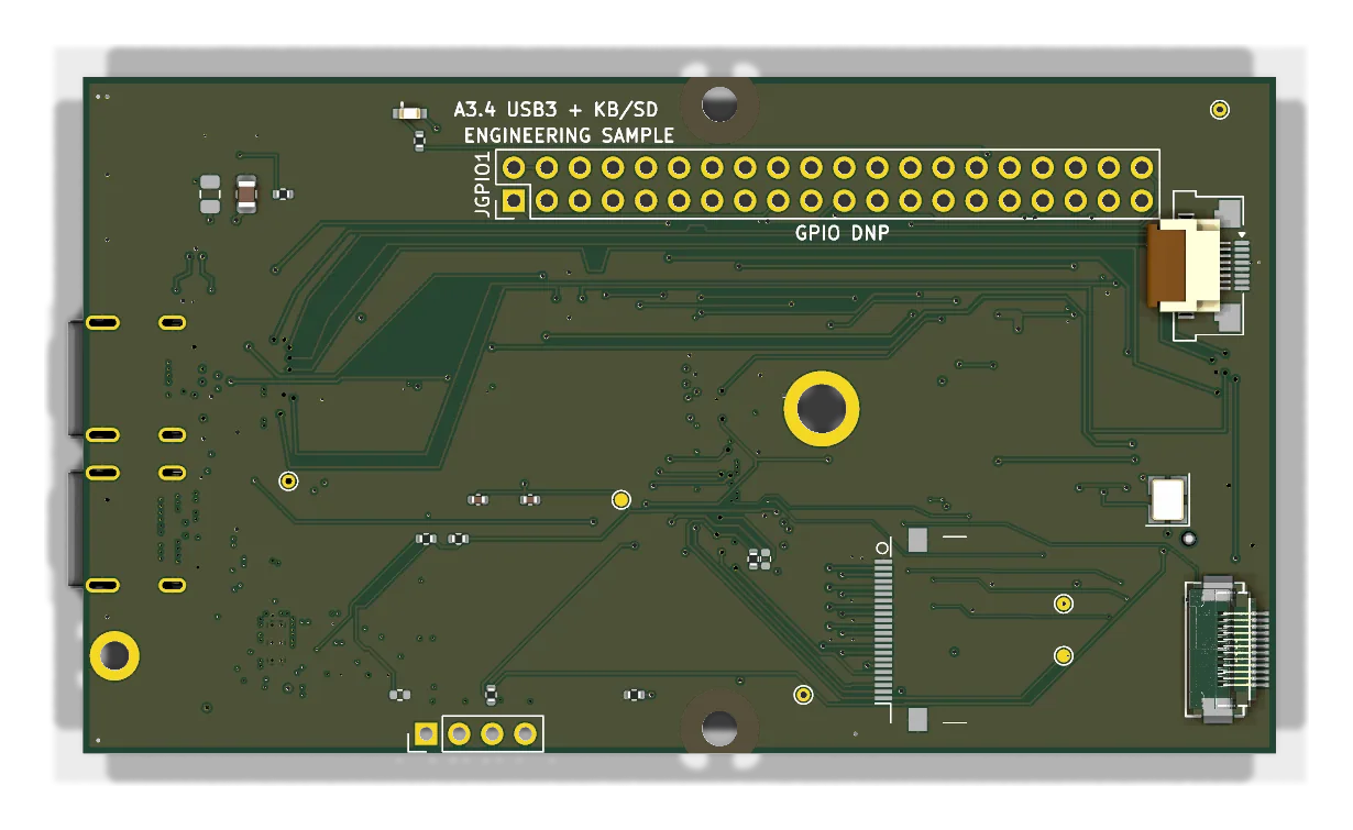
Sourcing fork of A3.4 that swaps the microSD FFC connector for a part the assembler actually stocks. Same footprint count; its value is the connector comparison.

Outline
91.69 × 52 mm
Layers
6 Cu
Footprints
63
Branch
main
Commit
fd66727
A3.4a perspective render

From A3.4

Notes Stocked microSD FFC
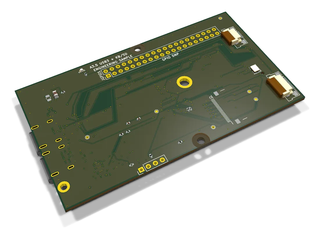
A3.5

Fabrication candidate

Electrical review closed A3 line · 91.69 × 52 mm

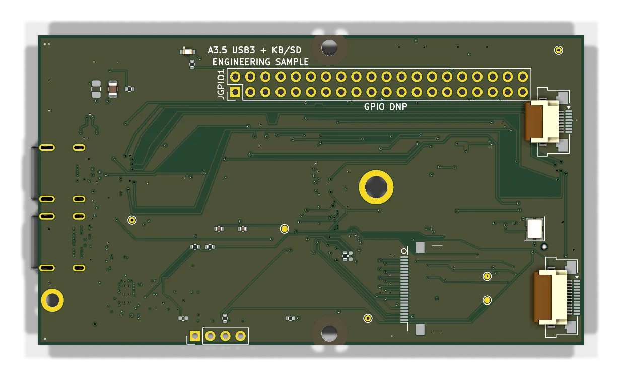
Closes the four findings raised against A3.4: an active-low VBUS switch matching the active-low attach signal, separate switched rails for the user port and keyboard, a corrected port strap, and every SuperSpeed pair re-routed to under 0.12 mm intra-pair skew with symmetric via counts.

Outline
91.69 × 52 mm
Layers
6 Cu
Footprints
67
Branch
main
Commit
8d63658
A3.5 perspective render

From A3.4

Continues as A3.6

Notes Electrical reviewReview closure
A3.6

Stocked Hirose microSD connector

Sourcing fork A3 line · 91.69 × 52 mm

Applies the stocked-connector change to the A3.5 baseline. The Hirose FH12 becomes the microSD flex connector used from here on.

Outline
91.69 × 52 mm
Layers
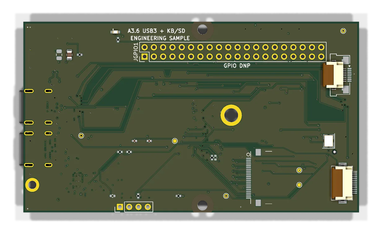
6 Cu
Footprints
67
Branch
main
Commit
54153e3
A3.6 perspective render
A3.7

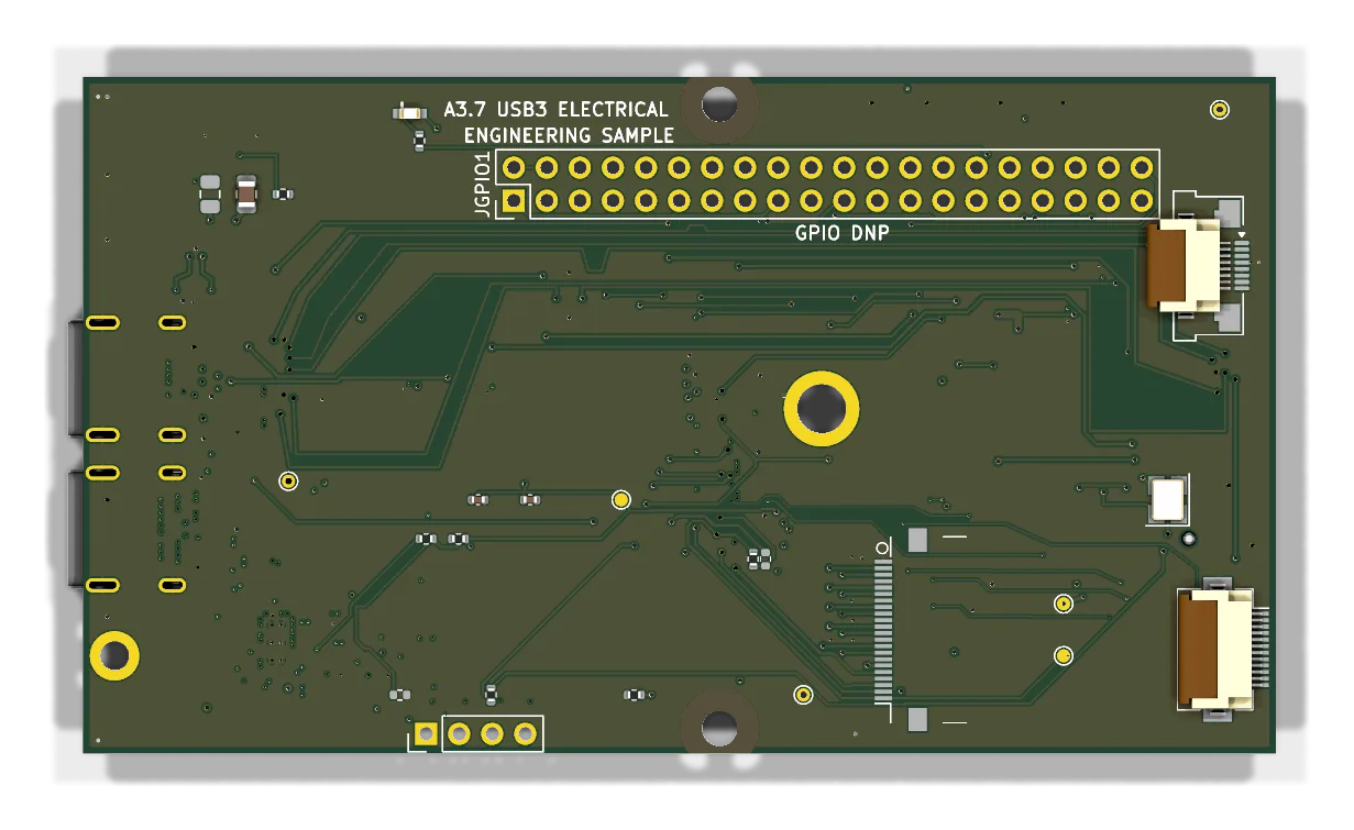
USB 3 electrical closure

USB 3 electrically closed A3 line · 91.69 × 52 mm

Sources the Type-C controller's 3.3 V rail, previously an unpowered net, and adds a fail-safe enable network so a missing 3.3 V domain cannot leave the controller enabled from 5 V alone. Also corrects the symbol's pin types, restoring ERC coverage on the most complex IC on the board.

Outline
91.69 × 52 mm
Layers
6 Cu
Footprints
72
Branch
main
Commit
d5cca76
A3.7 perspective render

From A3.6

Continues as A3.8

Notes USB 3 electrical closure
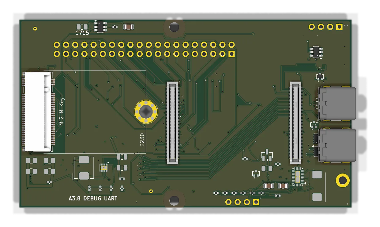
A3.8

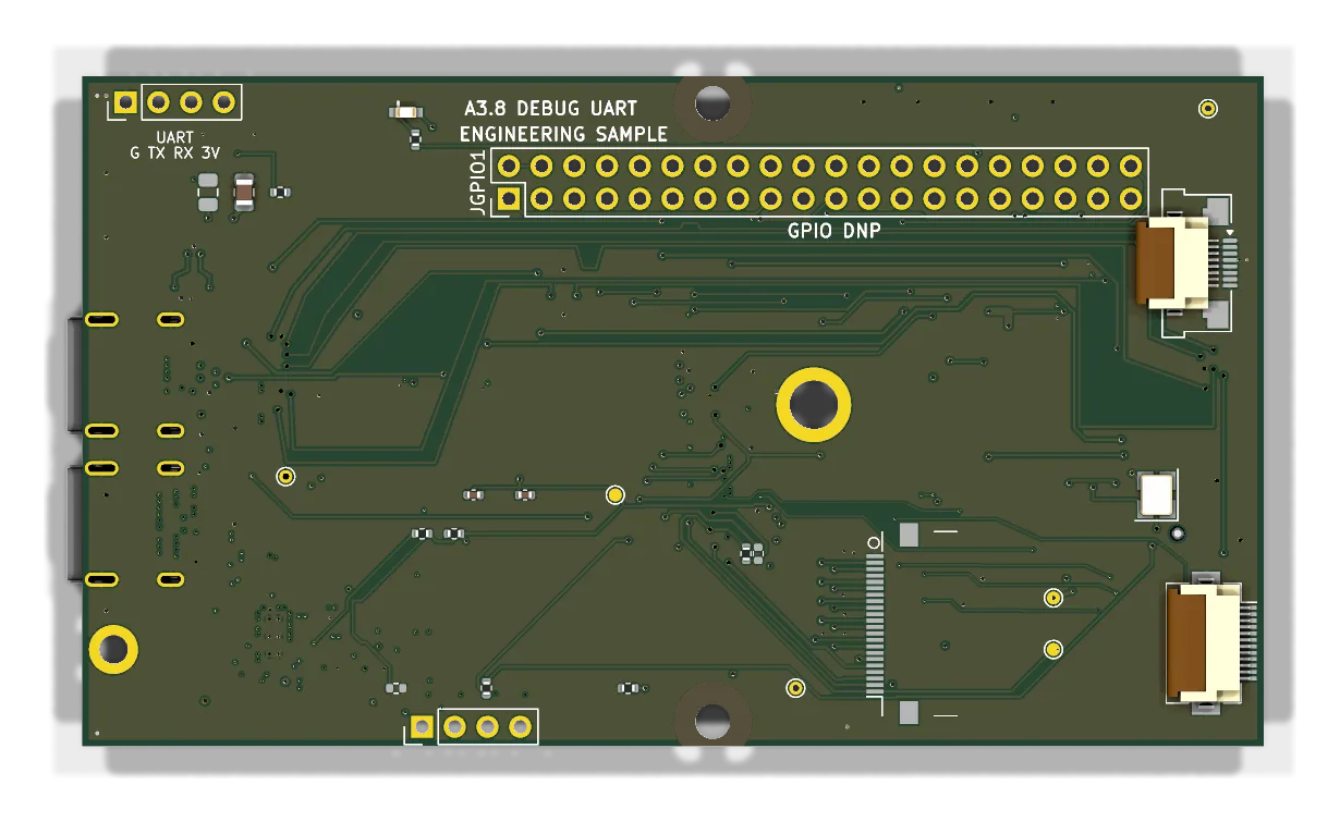
Debug UART

Debug UART added A3 line · 91.69 × 52 mm

Adds unpopulated debug UART holes. The highest footprint count of the A3 line, and the branch point for both the JLC upload chain and the daughter-card architecture.

Outline
91.69 × 52 mm
Layers
6 Cu
Footprints
73
Branch
main
Commit
4c87743
A3.8 perspective render
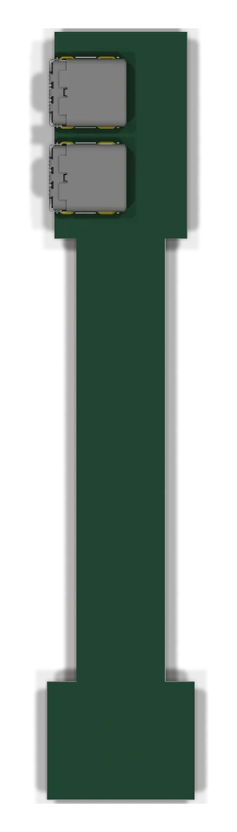
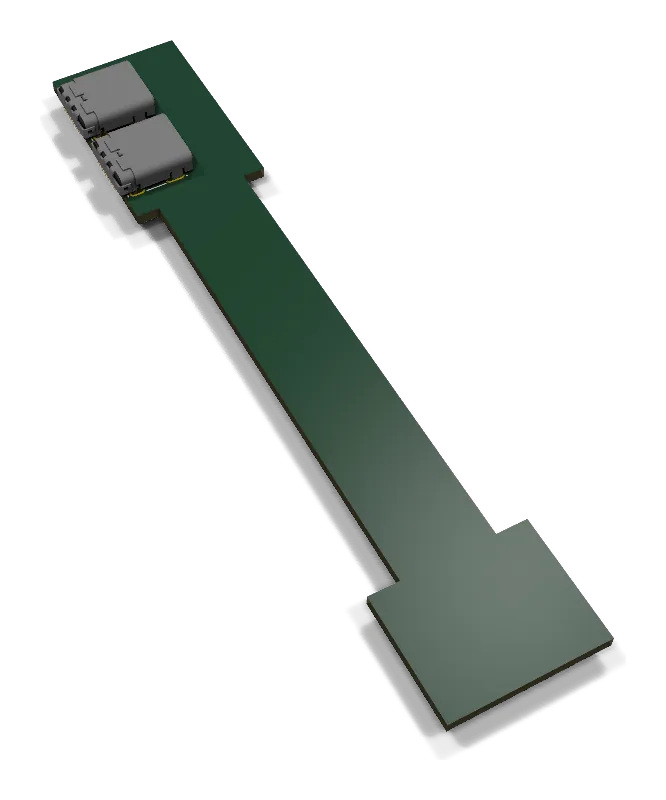
LH flex

Left-hand USB-C flex daughter card

Superseded Companion cards

The stiffened-flex approach to moving the USB-C ports off the carrier edge. Superseded by the rigid port card but retained in the tree.

Outline
20 × 104 mm
Layers
4 Cu
Footprints
3
Branch
main
Commit
6ff27fd
LH flex perspective render
A3.9

Left-hand USB-C daughter card

Architecture change A3 line · 91.69 × 52 mm

The largest structural change in the series. Both USB-C receptacles, the SuperSpeed mux, the ESD parts and every strap move to a separate left-hand port card reachable over a 31-way 0.3 mm FFC. Footprint count falls from 75 to 57 and only four host-side SuperSpeed signals cross the cable.

Outline
91.69 × 52 mm
Layers
6 Cu
Footprints
55
Envelope
7.42 mm populated
Branch
main
Commit
e8040b9
A3.9 perspective render

From A3.8

Continues as A3.10

Notes Daughter-card integrationCarrier integration handoff
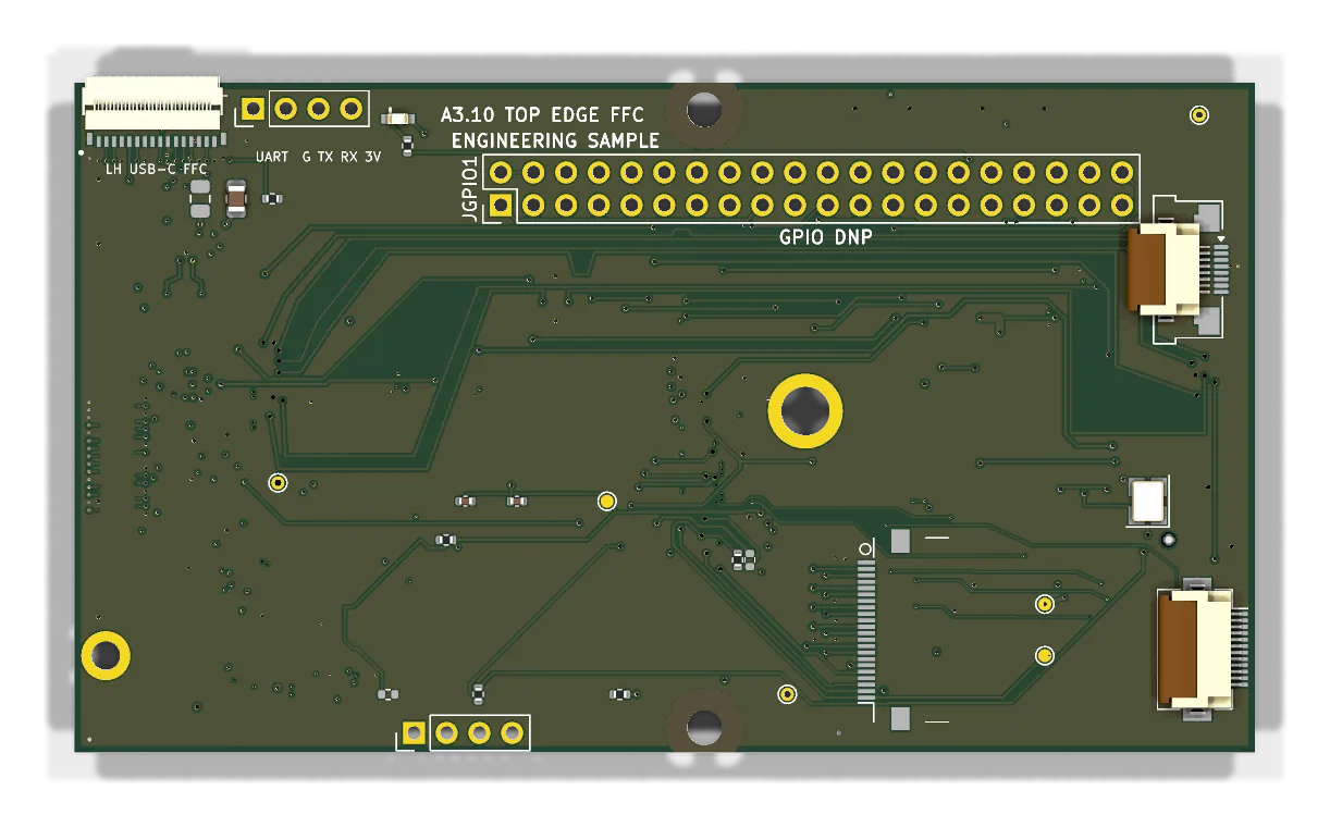
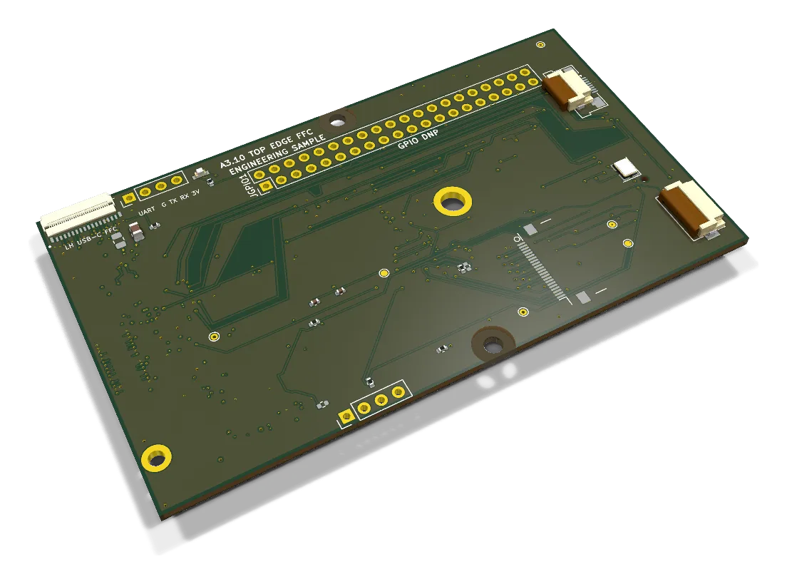
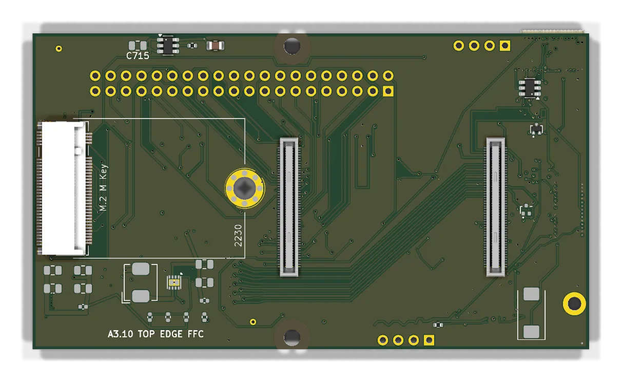
A3.10

Top-edge FFC placement

Placement study · routing gate fails A3 line · 91.69 × 52 mm

Demonstrates the straight top-edge cable path and replaces the generic connector proxy with Hirose's exact STEP model. Explicitly a placement study: the routing gate fails and no waiver was created.

Outline
91.69 × 52 mm
Layers
6 Cu
Footprints
55
Branch
main
Commit
d2f14c3
A3.10 perspective render
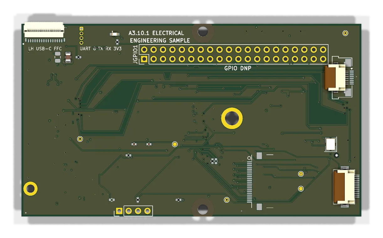
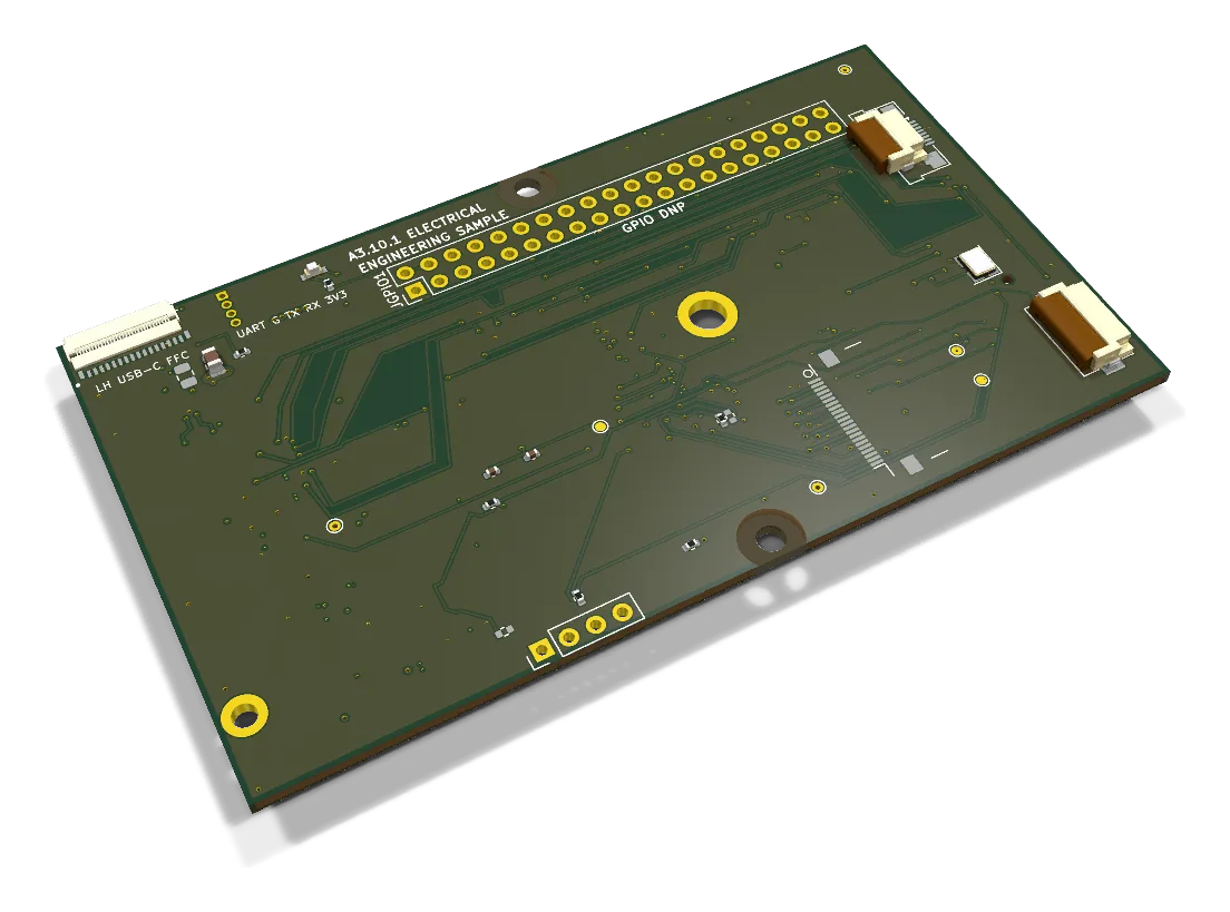
A3.10.1

Electrical closure and live quote

Live quote · sockets short A3 line · 91.69 × 52 mm

Closes A3.10's routing and is the first revision with a real assembler quote. The quote stalled at component matching because both CM5 socket rows were short.

Outline
91.69 × 52 mm
Layers
6 Cu
Footprints
56
Branch
main
Commit
f8b436c
A3.10.1 perspective render

From A3.10

Continues as A3.11.1

Notes Electrical closureCost reduction analysis
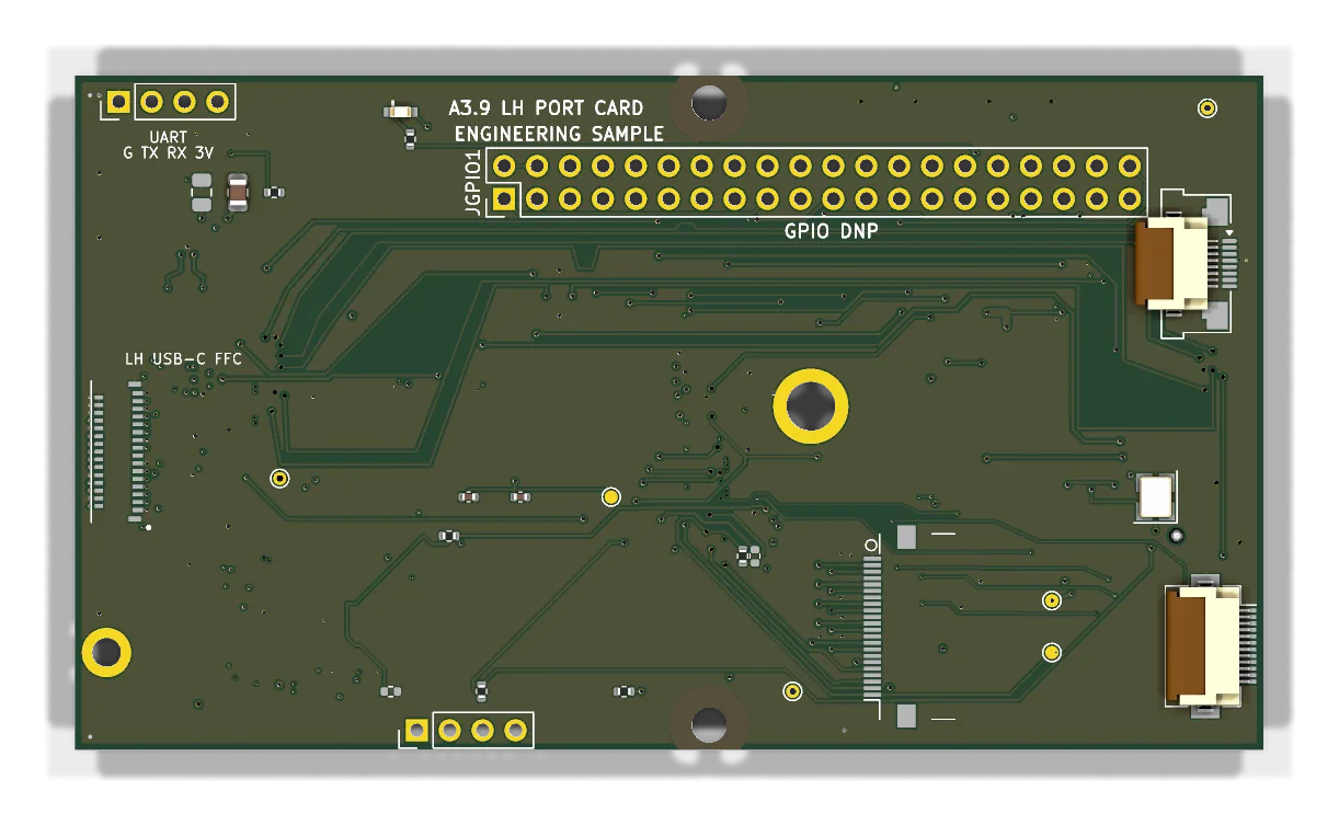
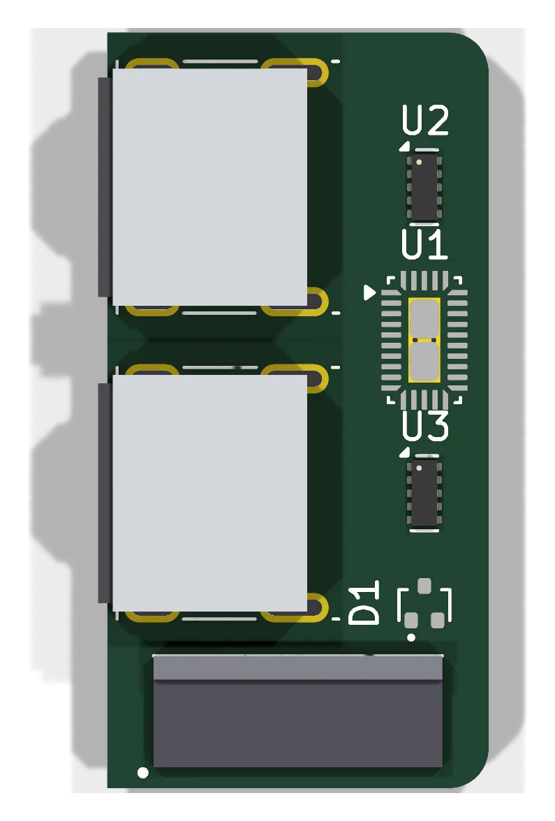
LH port card

Left-hand USB-C rigid port card

Companion card Companion cards

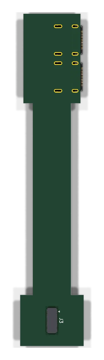
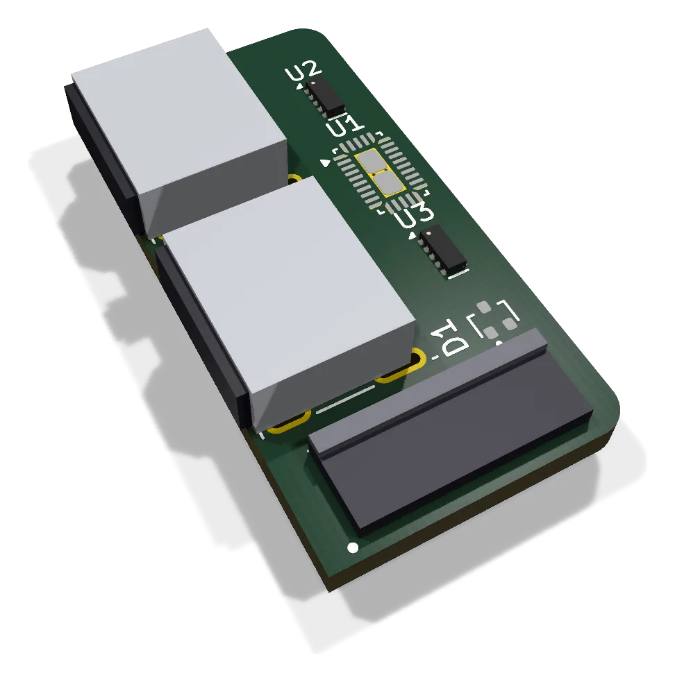
Rigid four-layer port card carrying both USB-C receptacles, the SuperSpeed mux and the ESD parts, reachable from the A3.9 carrier over a 31-way FFC. Orphaned when B2.6 brought the receptacles back onto the carrier.

Outline
14.4 × 28.53 mm
Layers
4 Cu
Footprints
7
Branch
main
Commit
e8040b9
LH port card perspective render
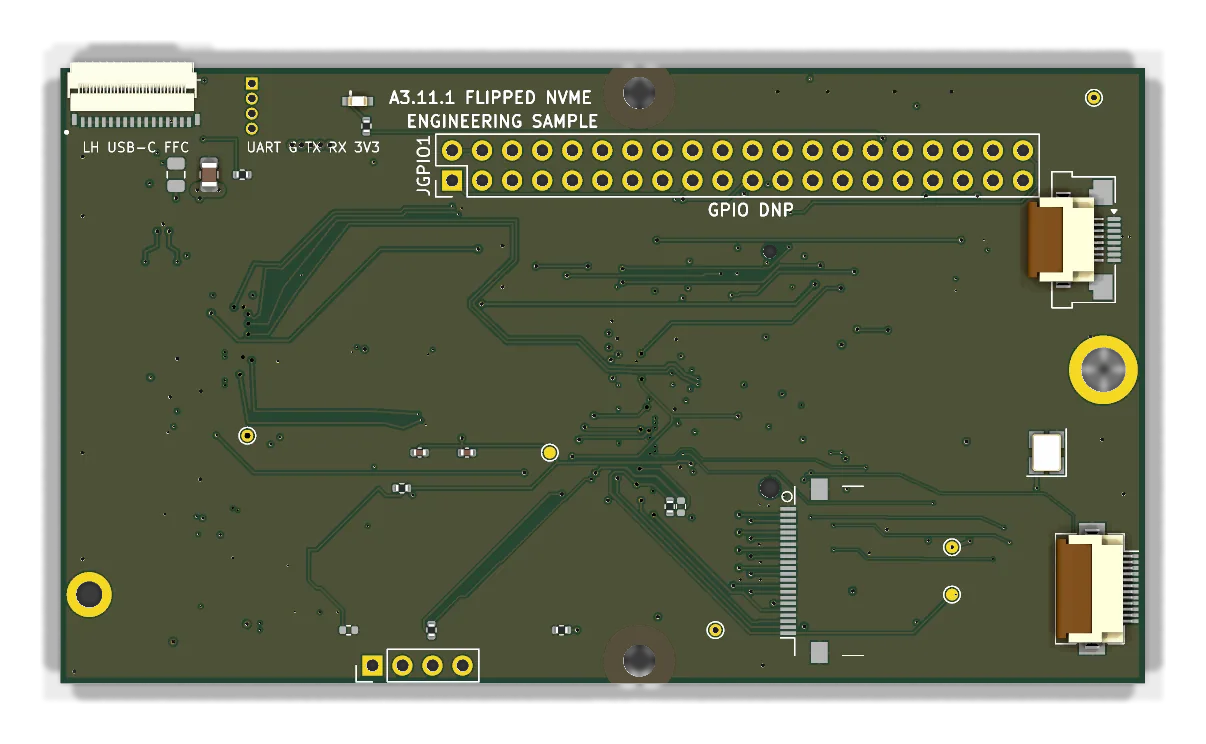
A3.11.1

Flipped NVMe closure

Head of merged A3 line A3 line · 91.69 × 52 mm

Flips the NVMe orientation and closes the resulting routing. Same outline, stack and footprint count as A3.10.1; the head of the merged daughter-card line.

Outline
91.69 × 52 mm
Layers
6 Cu
Footprints
56
Branch
main
Commit
4011984
A3.11.1 perspective render
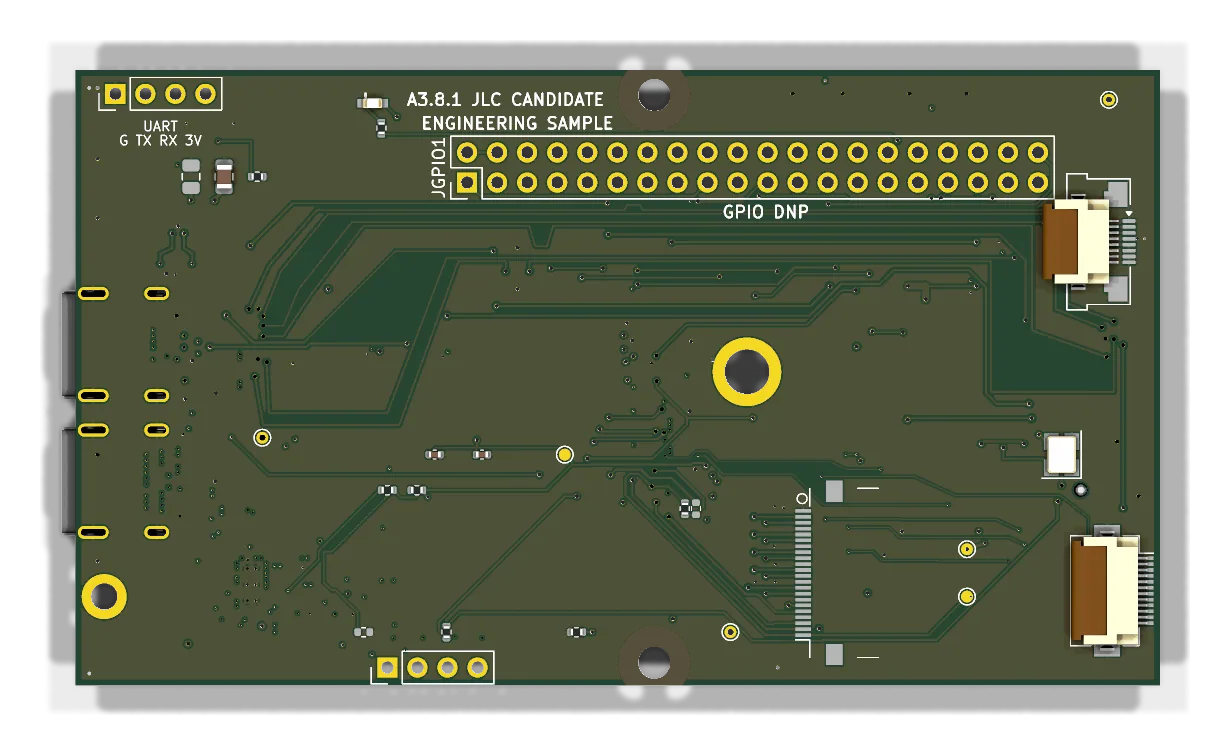
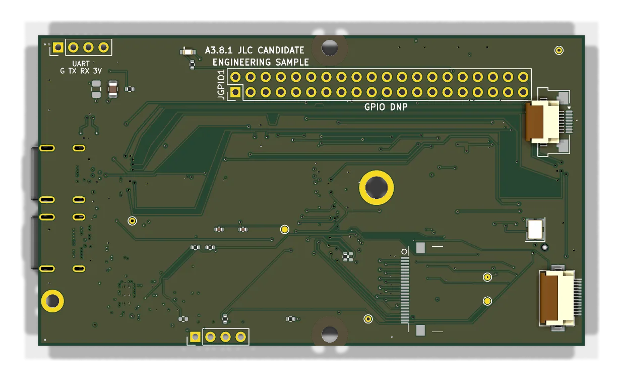
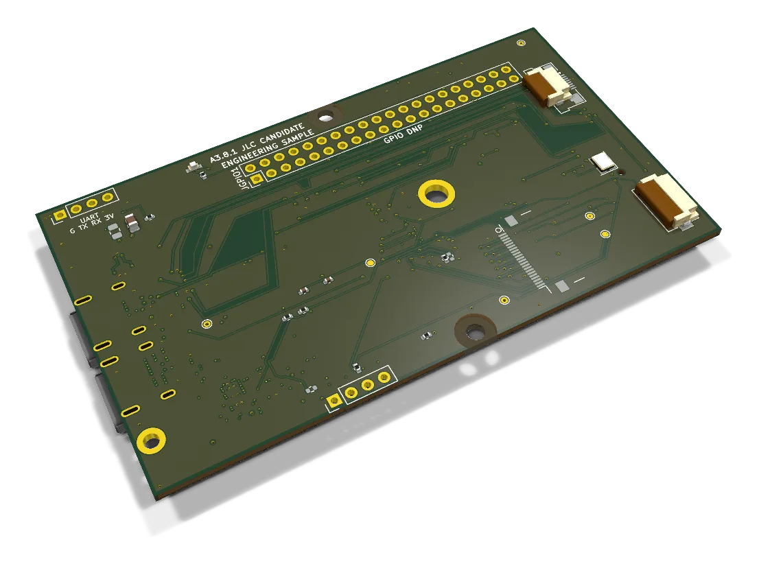
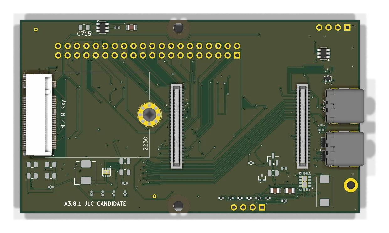
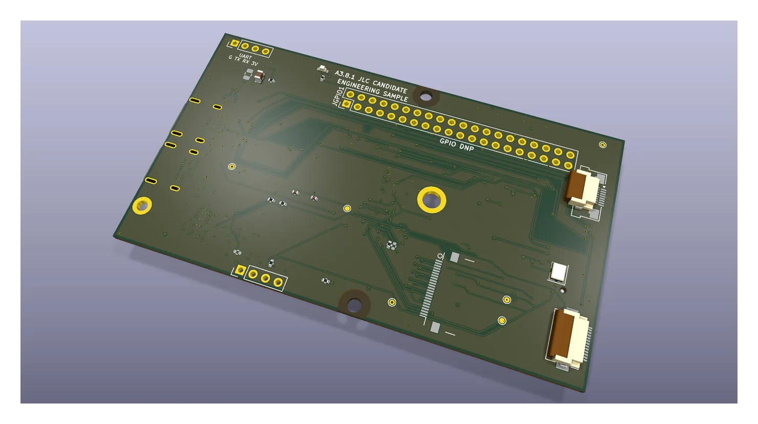
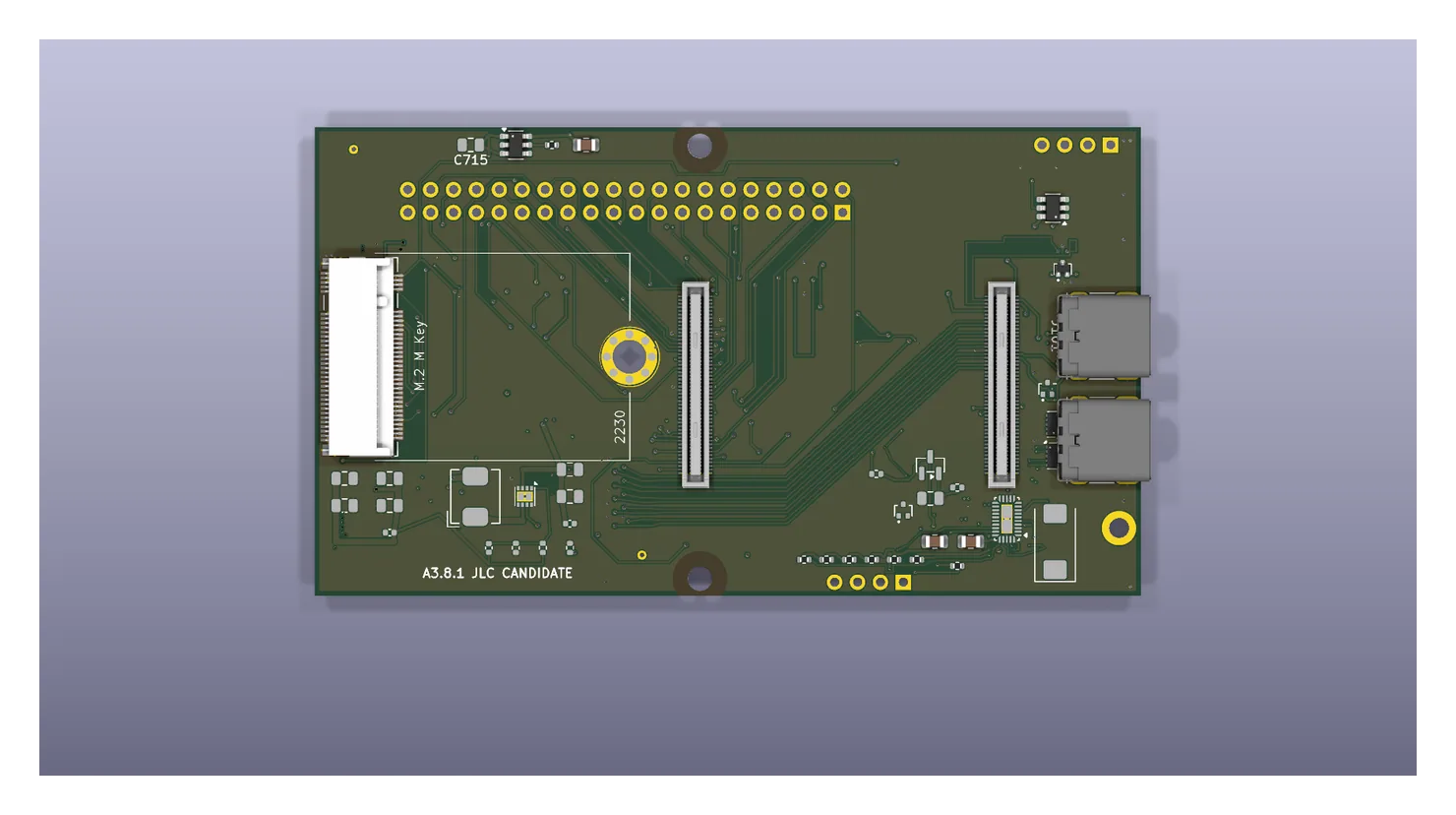
A3.8.1

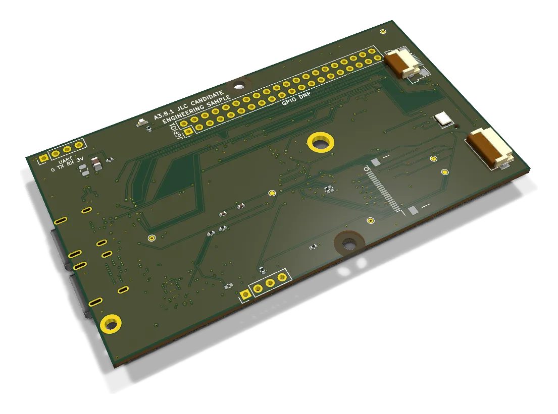
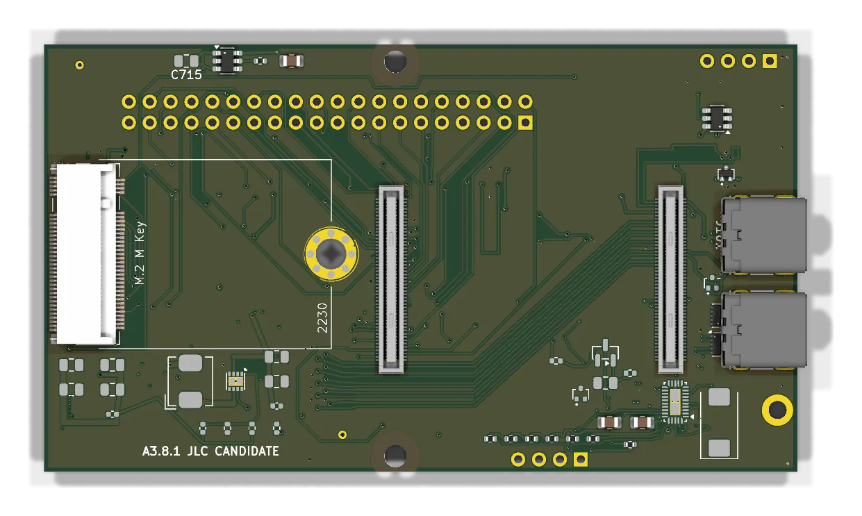
JLC closure

JLC closure A3 line · 91.69 × 52 mm

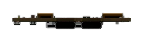
Power closure and assembler-facing corrections on the A3.8 board ahead of a quote.

Outline
91.69 × 52 mm
Layers
6 Cu
Footprints
73
Branch
main
Commit
8567200
A3.8.1 perspective render
A3.8.2

JLC BOM closure

JLC BOM closure A3 line · 91.69 × 52 mm

Bill-of-materials closure on the A3.8.1 artwork so every fitted part resolves to a stocked assembler part. Only its render set is kept on the main branch.

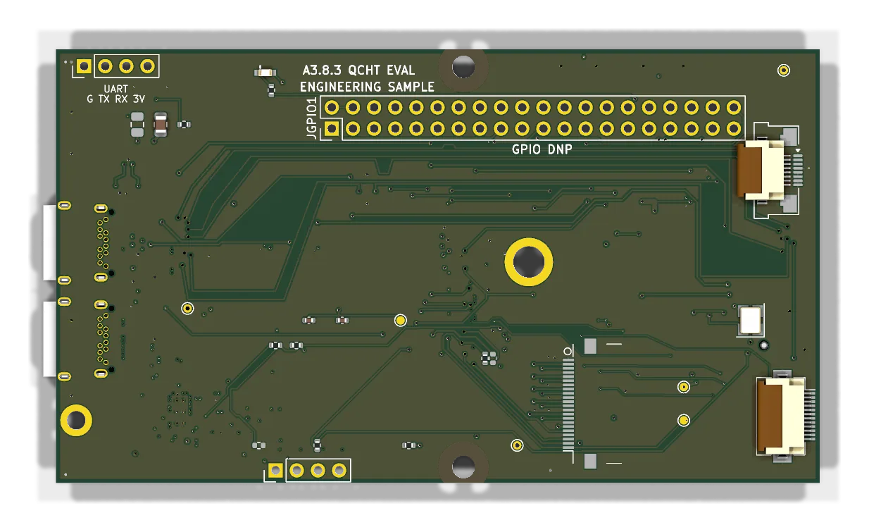
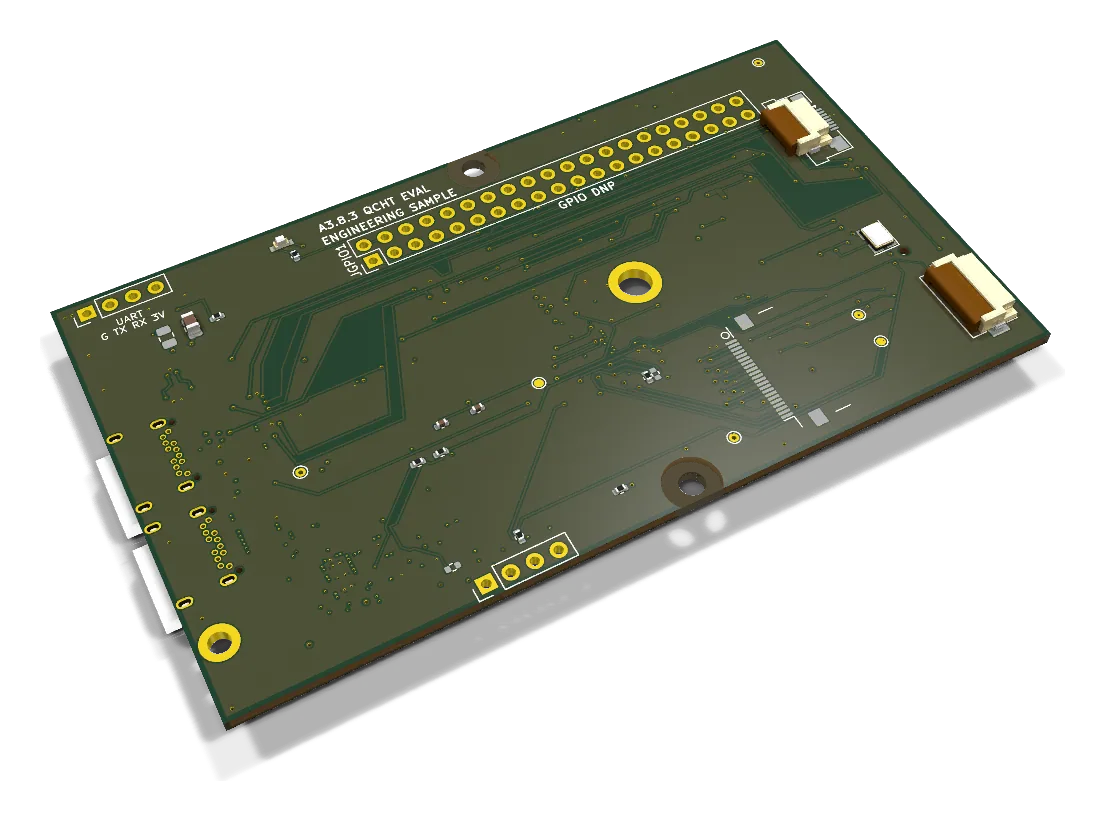
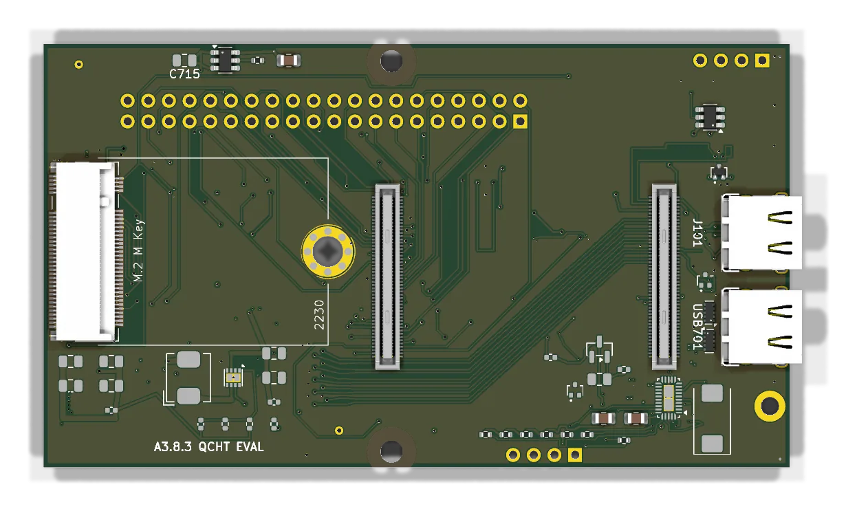
A3.8.3

Stocked QCHT USB-C evaluation

Connector evaluation A3 line · 91.69 × 52 mm

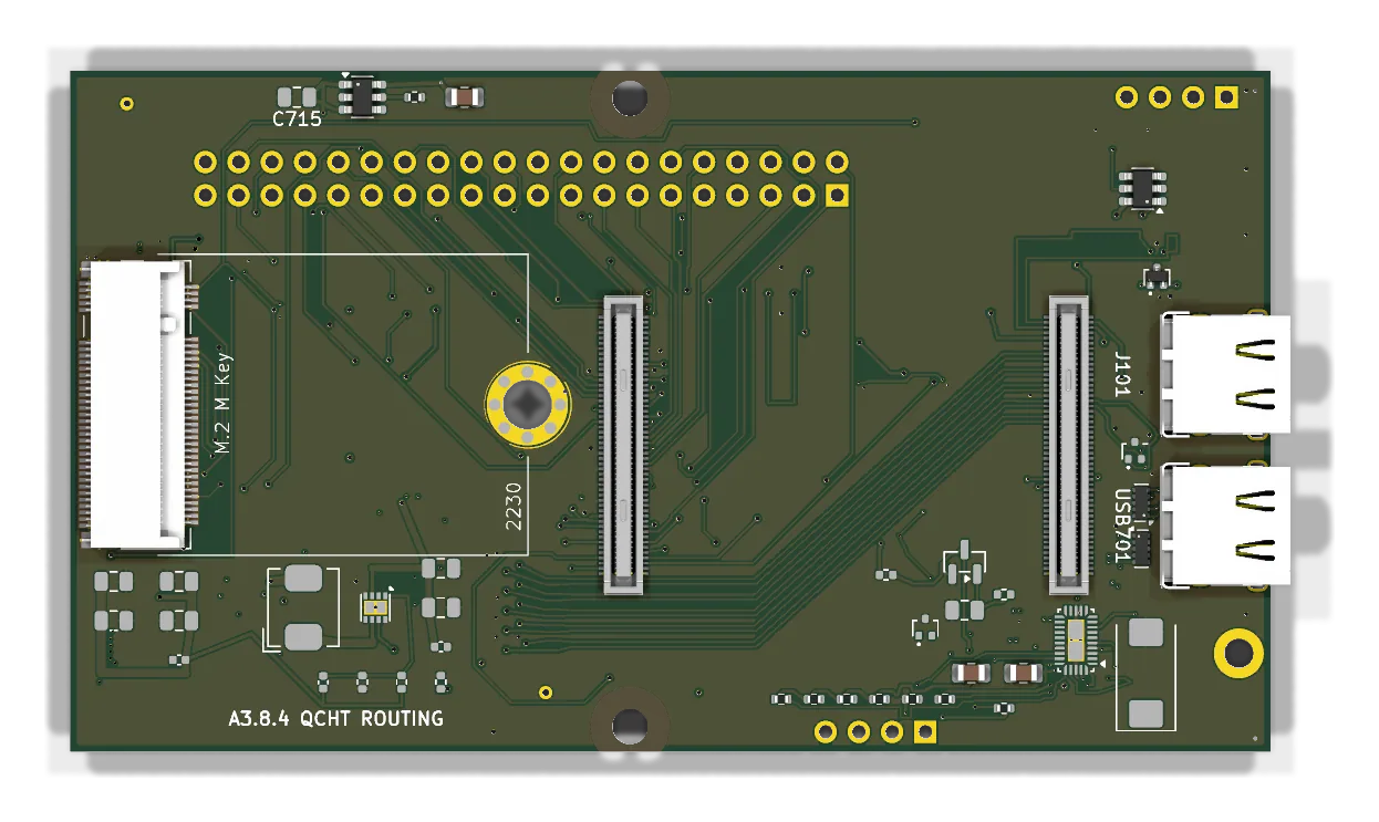
Evaluates a stocked SHOU HAN 24-pin USB-C receptacle at both Type-C positions using the supplier's exact footprint. Kept as a deliberately failing footprint-evaluation snapshot.

Outline
91.69 × 52 mm
Layers
6 Cu
Footprints
73
Branch
codex/a3.8.3-stocked-usbc
Commit
bd4a5def68
A3.8.3 perspective render
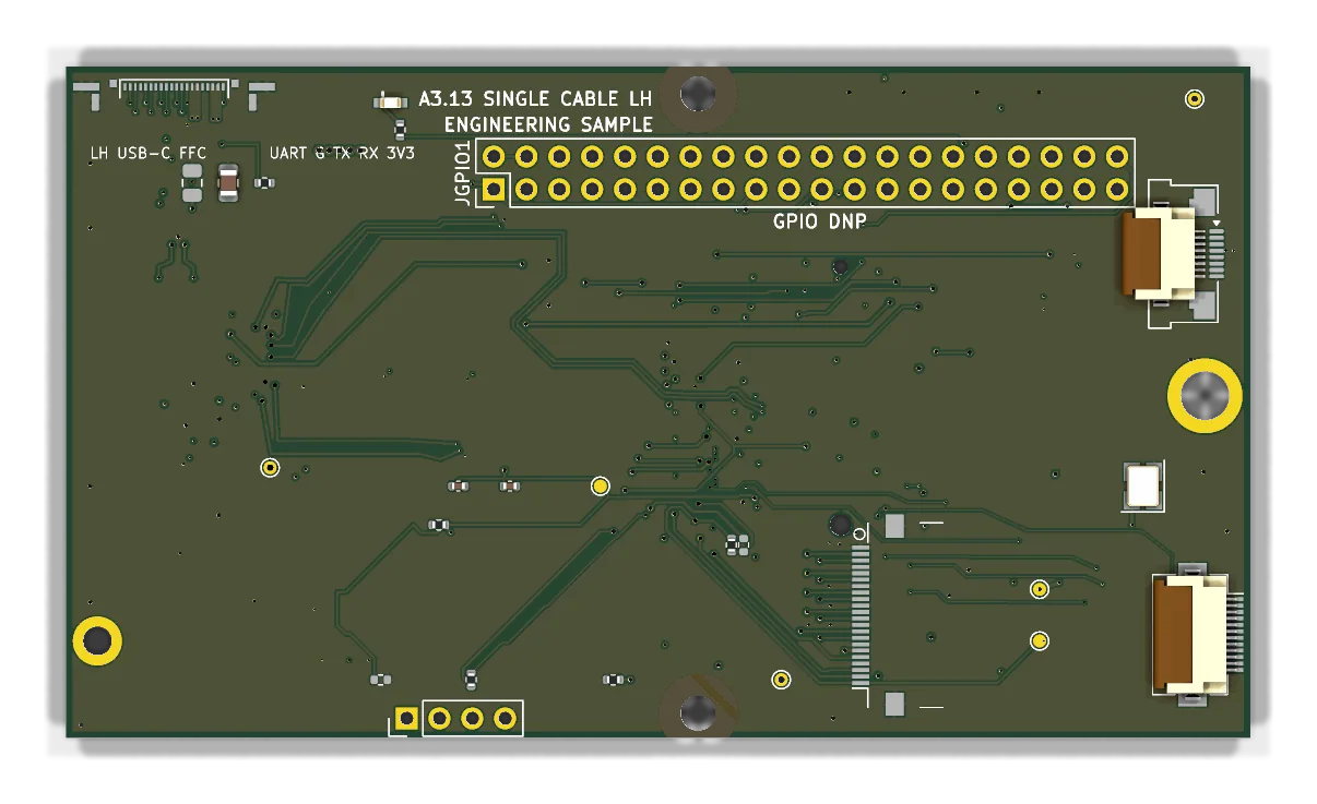
A3.13

Single-cable left-hand carrier

Unmerged work in progress A3 line · 91.69 × 52 mm

Replaces the 31-way signal FPC plus the four-way power harness with one 20-contact I-PEX CABLINE-CA-II interface to the port card, keeping the flipped M.2 socket. An engineering work in progress that never merged.

Outline
91.69 × 52 mm
Layers
6 Cu
Footprints
79
Branch
codex/a3.13-single-cable-lh
Commit
fac8f71de6
A3.13 perspective render
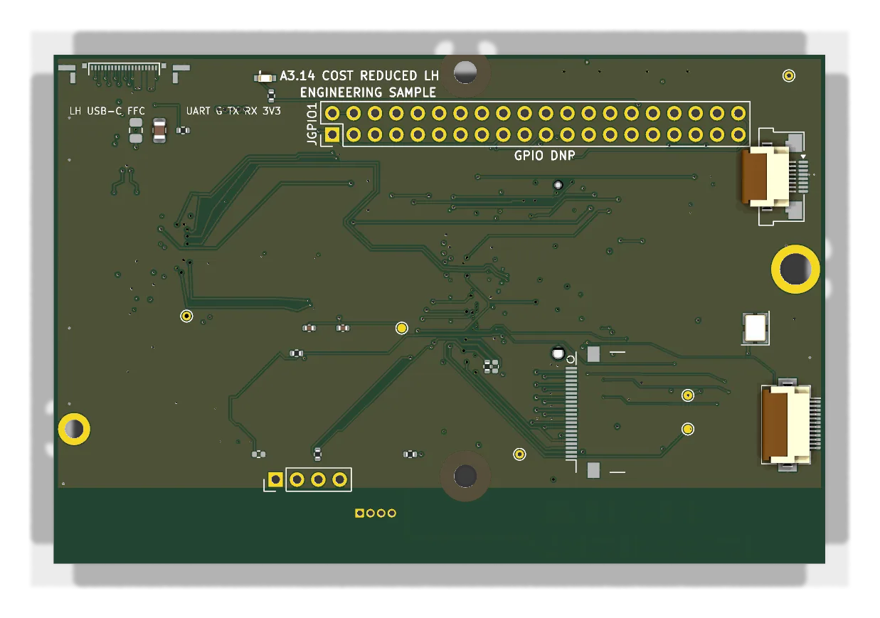
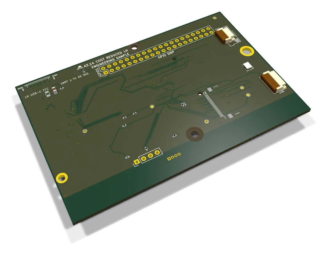
A3.14

Cost-reduced single-cable carrier

Unmerged work in progress A3 line · 91.69 × 52 mm

Applies the safe parts of the cost-reduction study to A3.13 and corrects an off-board PD stage and a mounting-hole crossing found visually. Supersedes A3.13's unmerged pull request.

Outline
91.69 × 60.5 mm
Layers
6 Cu
Footprints
79
Branch
codex/a3.14-cost-reduced-single-cable
Commit
f5438ce0e0
A3.14 perspective render

From A3.13

Notes Cost reduction analysis
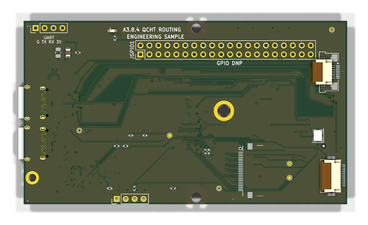
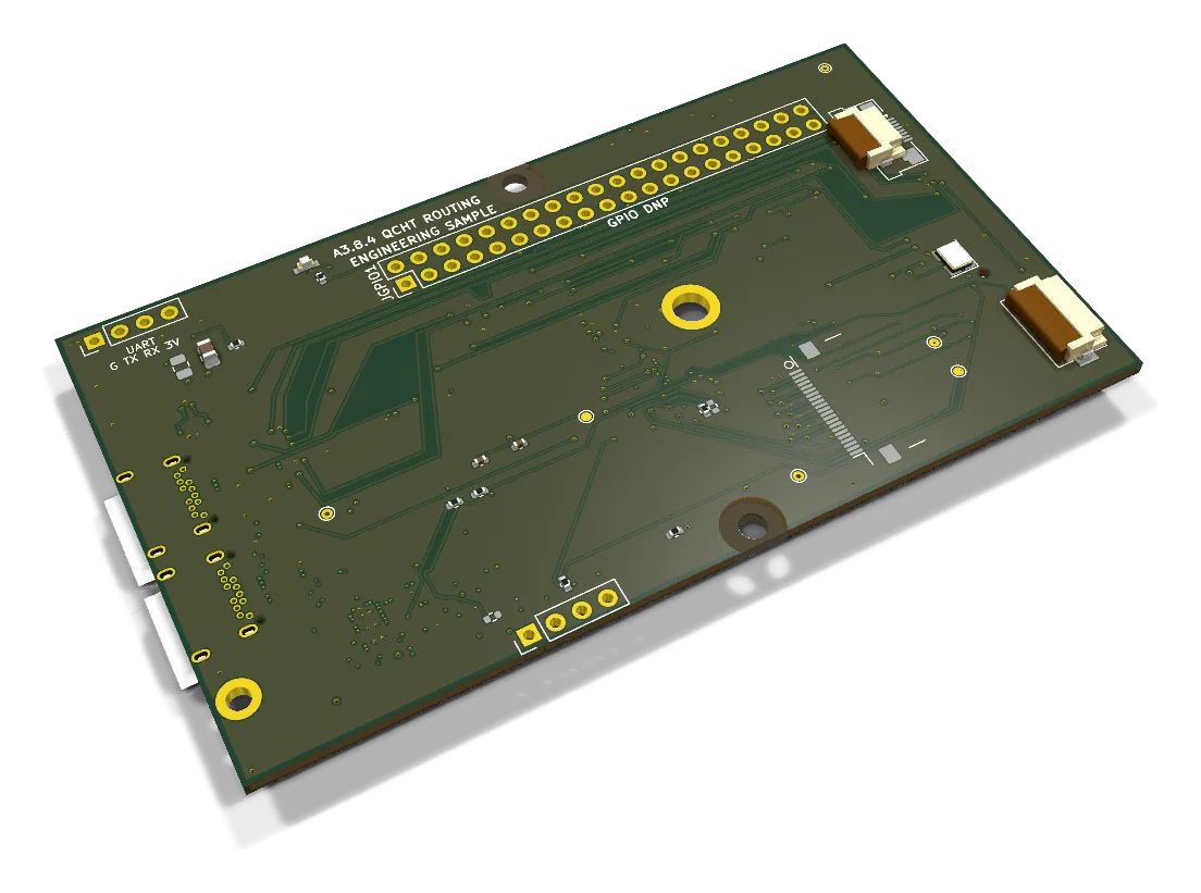
A3.8.4

QCHT-native routing closure

Rejected connector study A3 line · 91.69 × 52 mm

Completes a native fanout for the stocked QCHT receptacle at both USB-C positions. The connector was later rejected; B1 explicitly excludes it and the upload chain kept the Molex artwork.

Outline
91.69 × 52 mm
Layers
6 Cu
Footprints
73
Branch
codex/a3.8.4-qcht-routing
Commit
3d19b999e4
A3.8.4 perspective render
A3.8.5

JLC upload snapshot

Uploaded for quote A3 line · 91.69 × 52 mm

The upload snapshot: PCB and schematic hashes match the verified A3.8.1/A3.8.2 Molex USB-C artwork. Both the B1 assembly experiment and the VBUS correction chain fork from here.

Outline
91.69 × 52 mm
Layers
6 Cu
Footprints
73
Branch
main
Commit
3d9fbcd
A3.8.5 perspective render
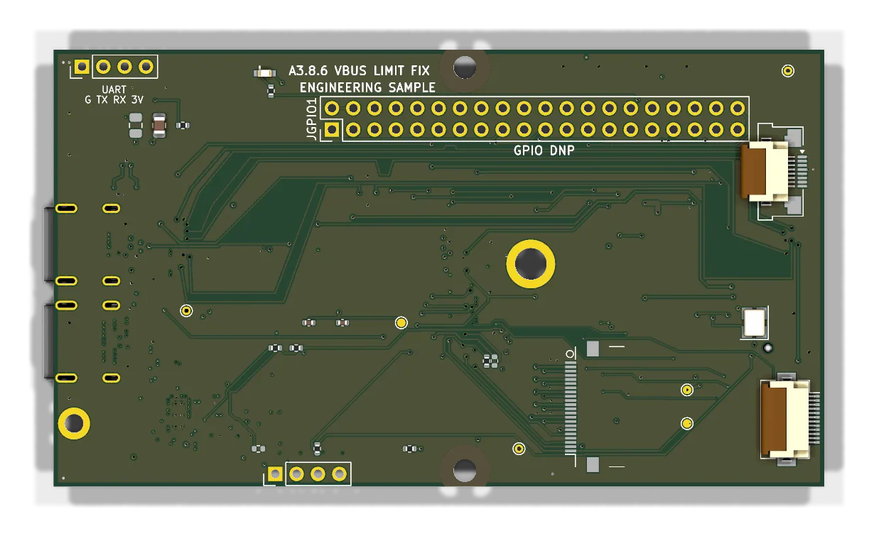
A3.8.6

VBUS current-limit correction

Electrical correction A3 line · 91.69 × 52 mm

Preserves the A3.8.5 placement, routing and stack and changes only two current-limit resistors, lifting the user USB-C VBUS switch above the controller's default SuperSpeed advertisement and restoring the keyboard rail's limit.

Outline
91.69 × 52 mm
Layers
6 Cu
Footprints
73
Branch
codex/a3.8.6-vbus-limit-correction
Commit
6755649d66
A3.8.6 perspective render
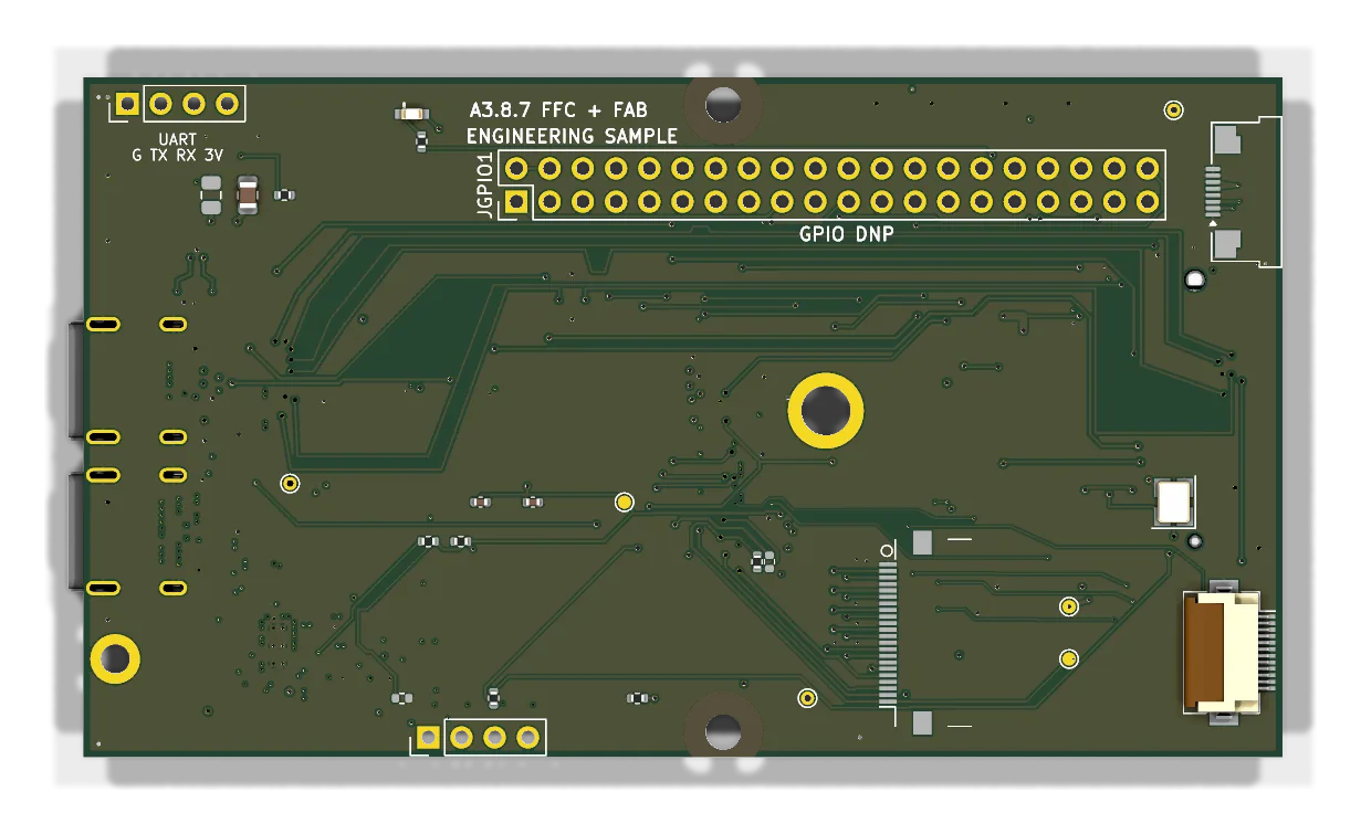
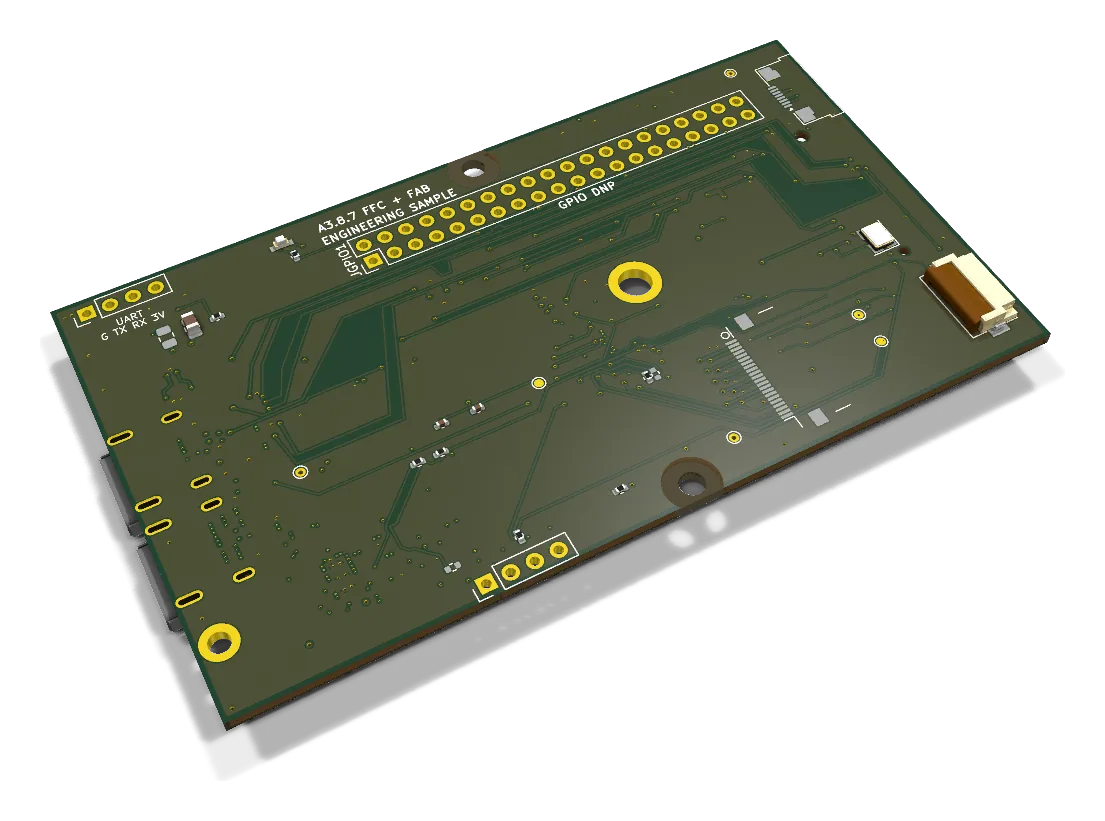
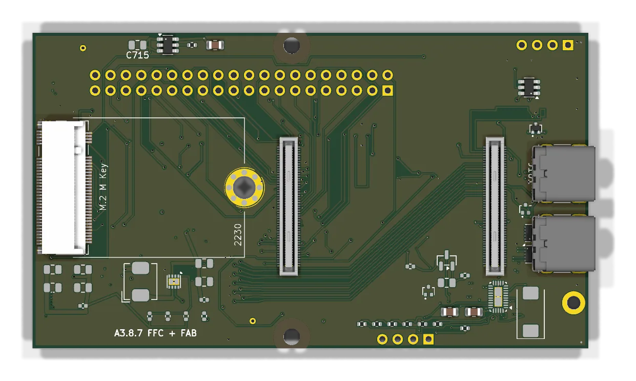
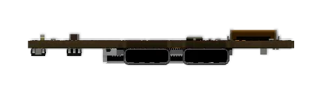
A3.8.7

Connector and fabrication correction — the fabricated board

Fabricated · 5 boards received A3 line · 91.69 × 52 mm fabricatedbring-up

The revision that actually went to the board house: the A3.8.6 electrical state with the right-edge USB/keyboard FFC rotated to face the board edge and the manufacturing handoff corrected. Five boards came back on 2026-08-18. First bench bring-up booted a CM5 from eMMC through the carrier's USB-C power path; the physical return logged a backward SD FFC and an NVMe growing across the board, both corrected in the B2 line. Its display FFC must not be connected to an LCD.

Outline
91.69 × 52 mm
Layers
6 Cu
Footprints
73
Branch
codex/a3.8.7-connector-fab-correction
Commit
c4ed9d83ff
A3.8.7 perspective render
Notes Field return evidence
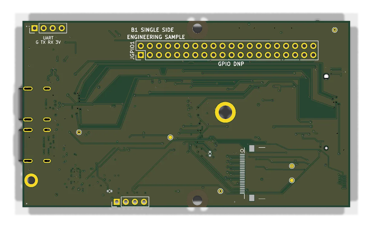
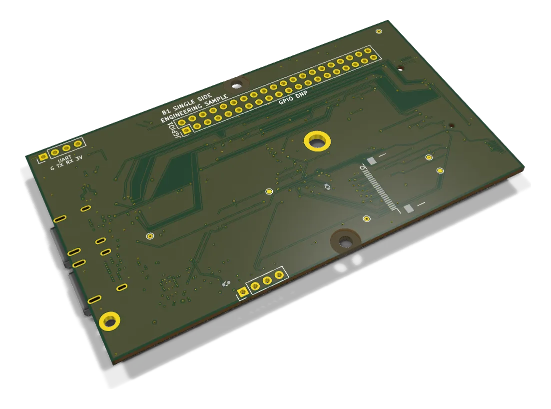
B1

Single-sided assembly prototype

Assembly prototype B1 · assembly experiment

An immutable major-revision fork of the A3.8.5 upload snapshot aimed at bottom-only production assembly while keeping both CM5 sockets, the M.2 interface, the two Molex USB-C ports and the fitted breakouts. The last revision to carry the 91.69 × 52 mm landscape outline.

Outline
91.69 × 52 mm
Layers
6 Cu
Footprints
73
Branch
main
Commit
dd1931d
B1 perspective render
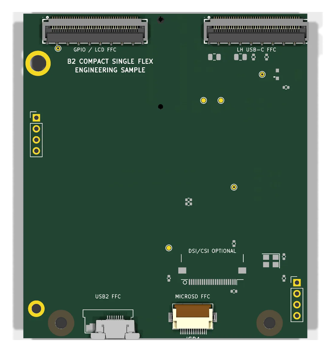
B2.0

Compact single-FFC architecture fork

Architecture fork · unrouted B2 line · compact portrait

Fresh architecture fork of A3.8.6: the outline goes portrait at exactly the OEM logic board's 65.4 × 74.8 mm footprint, both carrier-mounted USB-C receptacles leave the board, and their interface collapses into one 40-position shielded FFC toward a left-hand companion card. Deliberately unrouted.

Outline
65.4 × 74.8 mm
Layers
6 Cu
Footprints
55
Branch
main
Commit
d886956
B2.0 perspective render

From A3.8.6

Continues as B2.1

Notes B2 compact single-FFC checkpointBottom I/O and GPIO/LCD FFC
B2.1

Routed single-FFC carrier

Routed B2 line · compact portrait

Routes the B2.0 floorplan; the outline settles at 65.4 × 75.5 mm. First print-model fit study of the portrait shape.

Outline
65.4 × 75.5 mm
Layers
6 Cu
Footprints
55
Branch
main
Commit
6df2f63
B2.1 perspective render
B2.2

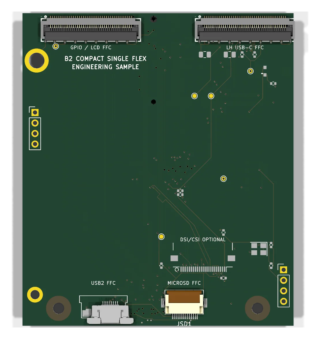
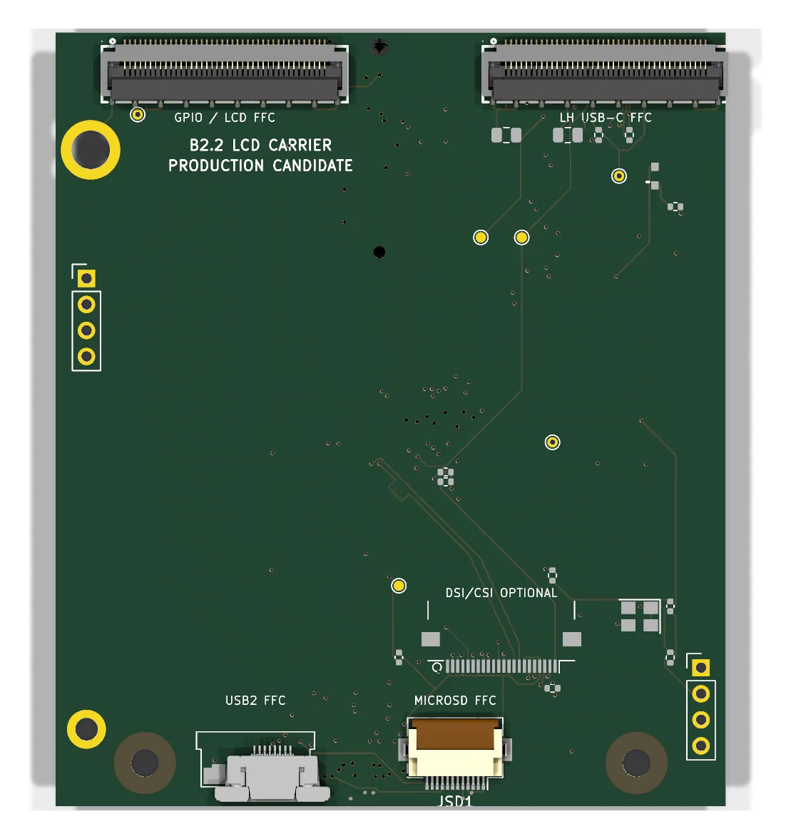
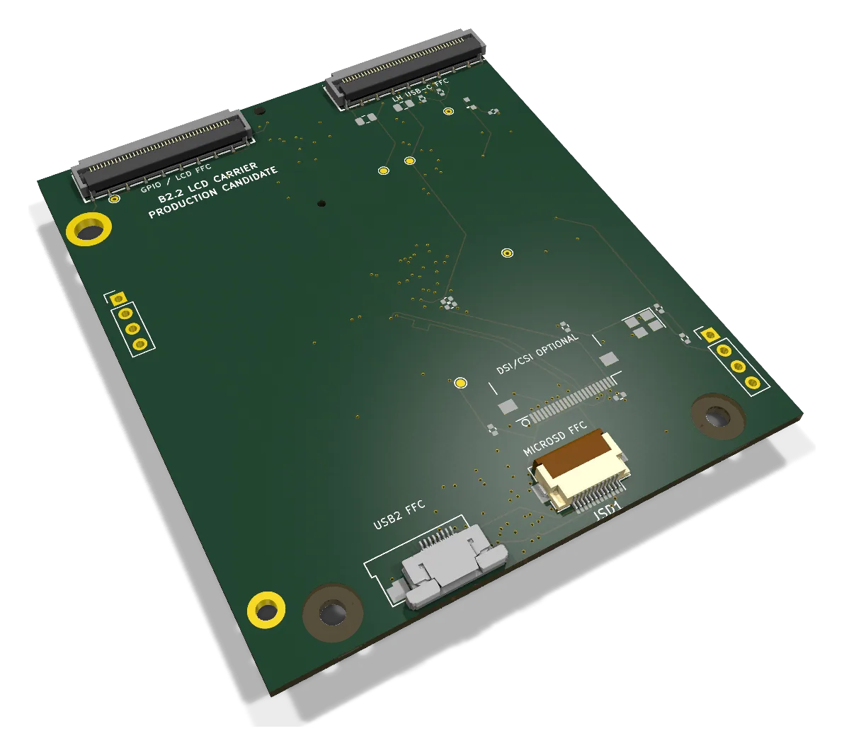
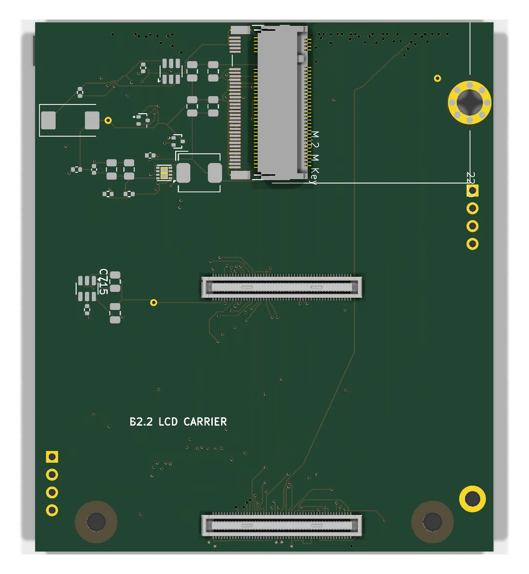
LCD interface production revision

LCD interconnect revision B2 line · compact portrait Koyomi contract

Fabrication-ready successor for the display link: the display FFC gains the repurposed panel-ID and insertion contacts that the Koyomi LCD R2.6 contract verifies against.

Outline
65.4 × 75.5 mm
Layers
6 Cu
Footprints
55
Branch
main
Commit
9be6dfa
B2.2 perspective render
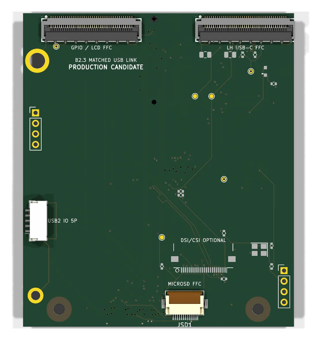
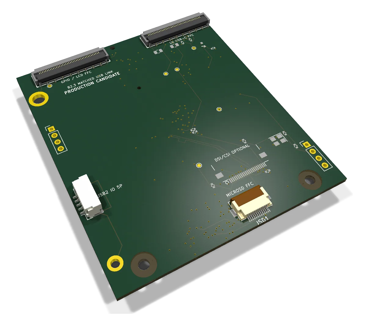
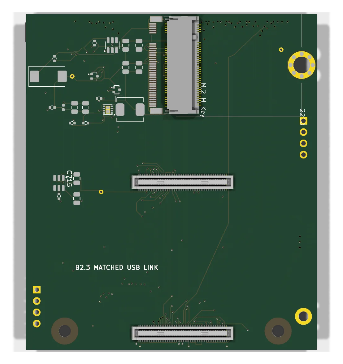
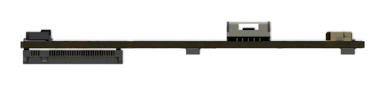
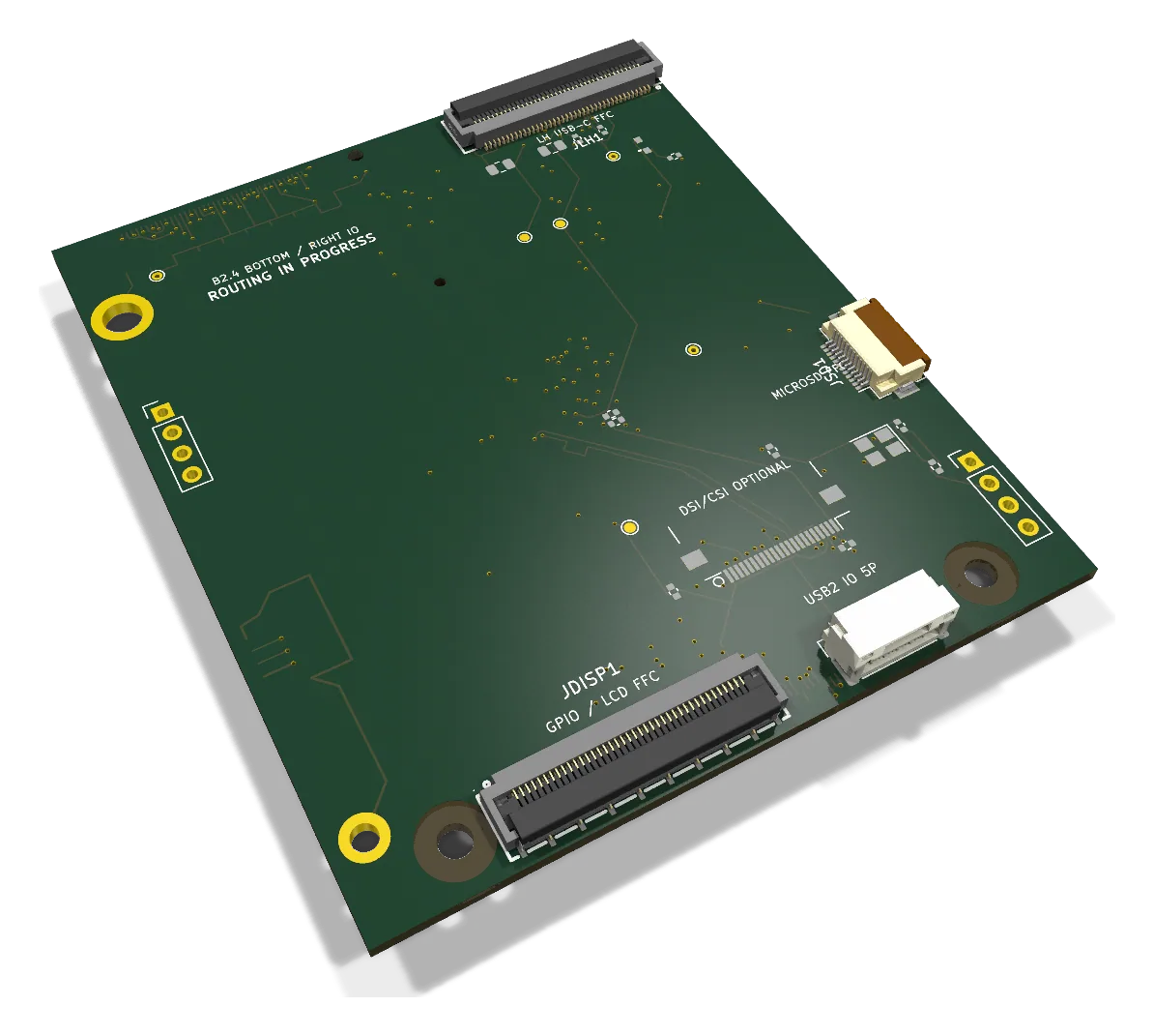
B2.3

Matching USB interconnect

Interconnect contract match B2 line · compact portrait

The USB 2.0 breakout connector becomes the exact JST GH part with the pin order that mates the I/O breakout board straight through, so no custom harness is needed.

Outline
65.4 × 75.5 mm
Layers
6 Cu
Footprints
55
Branch
main
Commit
f2052d3
B2.3 perspective render
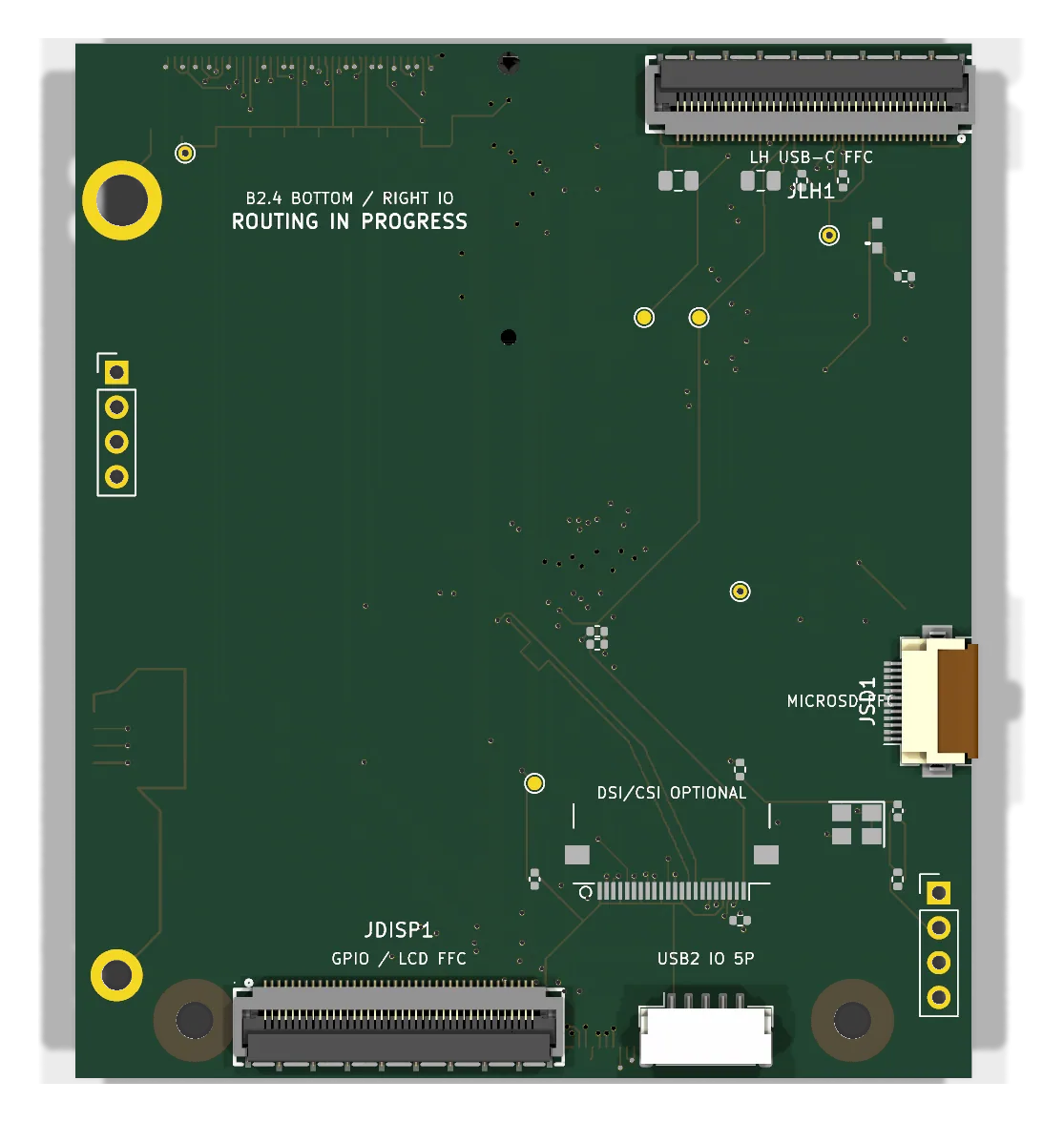
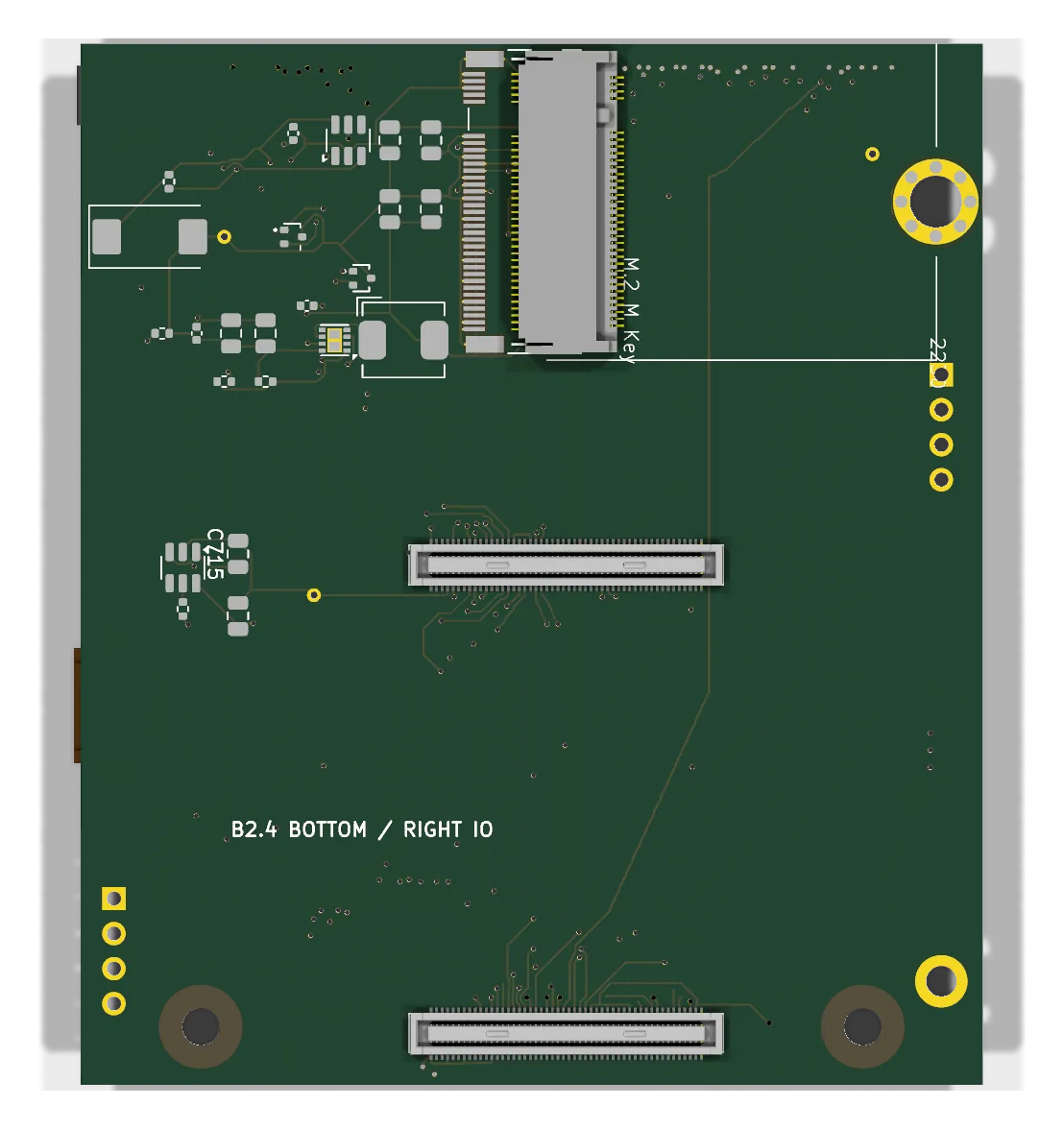
B2.4

Bottom-edge connectors

Routing checkpoint B2 line · compact portrait

Moves the cable interfaces to their requested chassis edges and reverses the SD FFC by 180°, the correction the A3.8.7 physical return later proved necessary. A routing-in-progress checkpoint.

Outline
65.4 × 75.5 mm
Layers
6 Cu
Footprints
55
Branch
main
Commit
a1b5bf6
B2.4 perspective render
B2.5

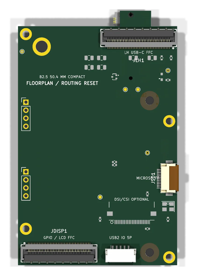
Rotated CM5, 15 mm narrower

Compact floorplan B2 line · compact portrait

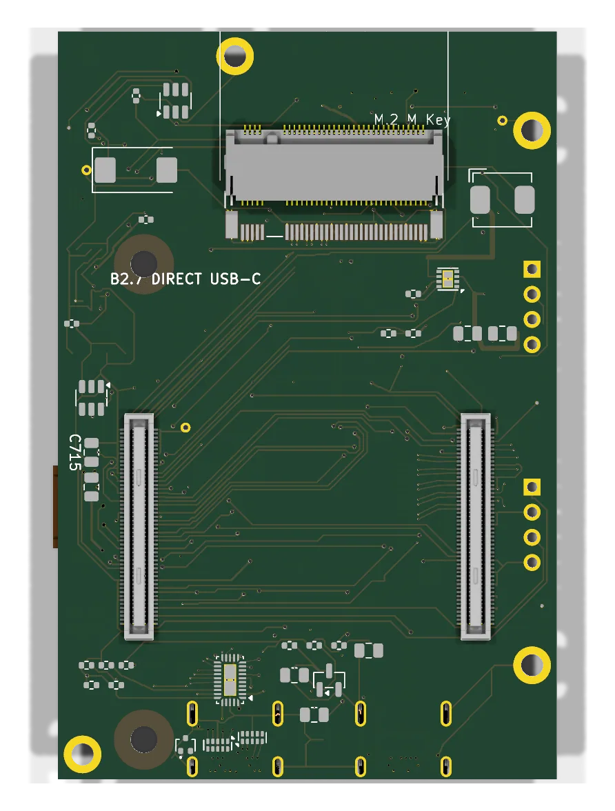
Removes 15 mm from the short edge by rotating the CM5 arrangement; a small top-edge tab carries the full M.2 land pattern, giving a 50.4 × 80.4 mm bounding envelope.

Outline
50.4 × 80.4 mm
Layers
6 Cu
Footprints
58
Branch
main
Commit
1b889db
B2.5 perspective render
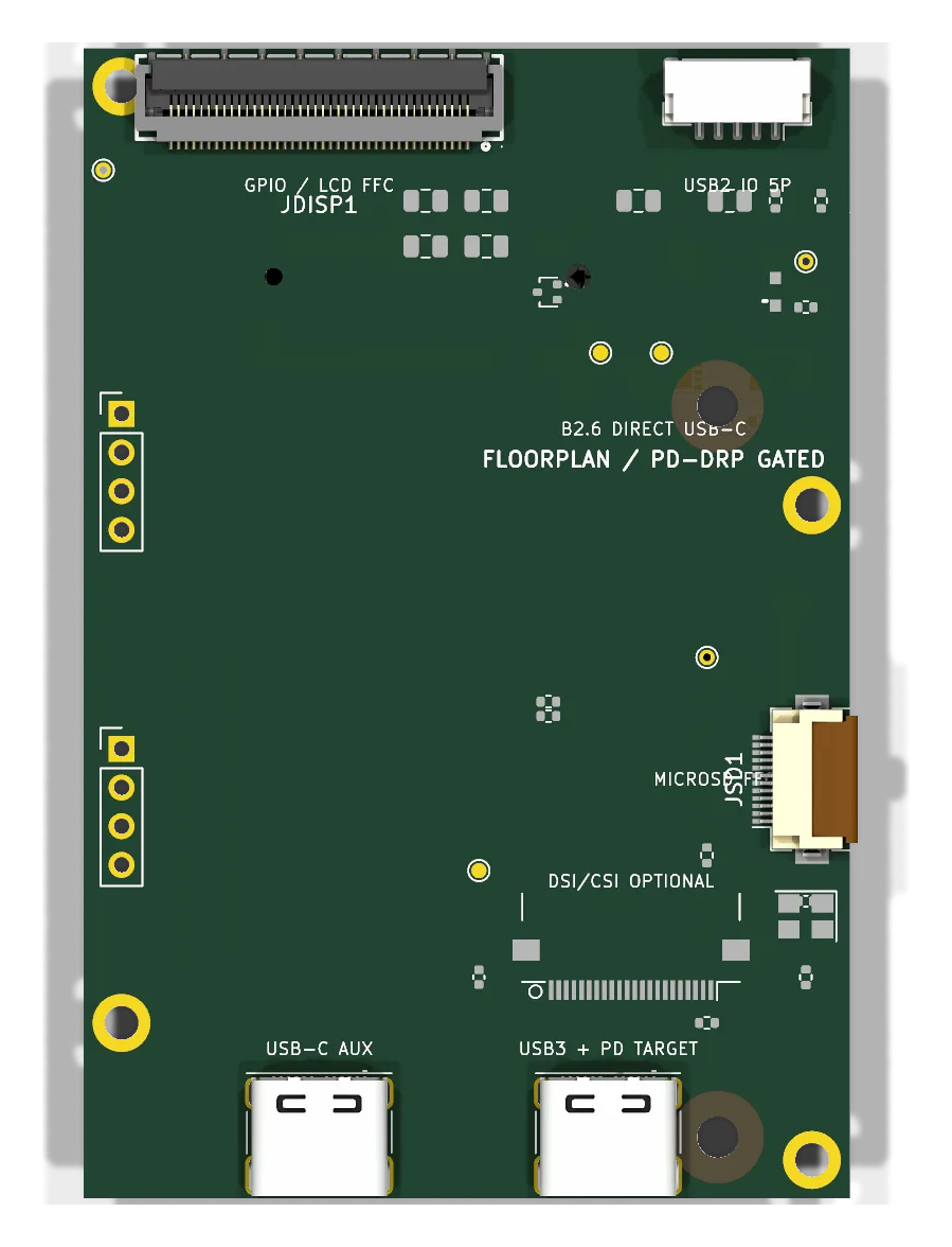
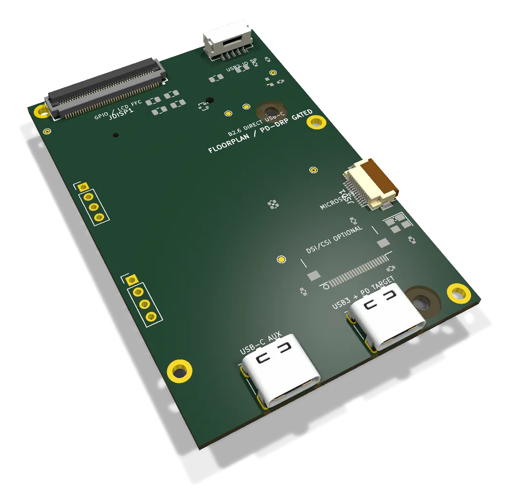
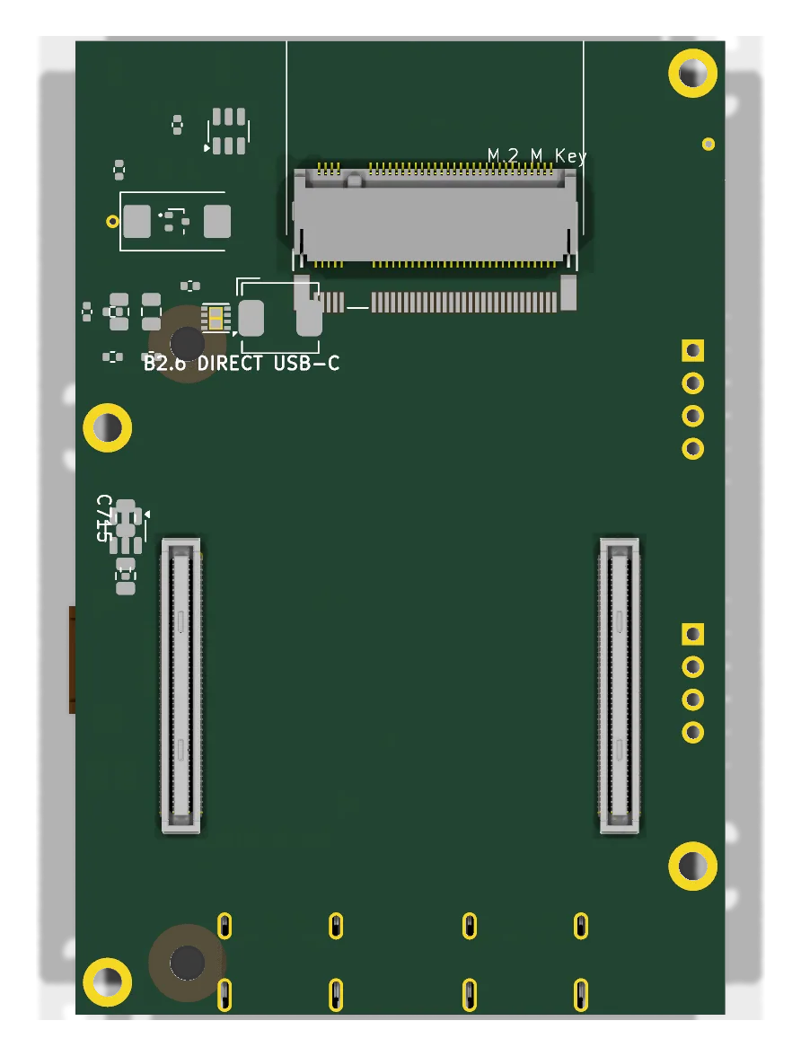
B2.6

Dual direct USB-C, left NVMe

Mechanical floorplan checkpoint B2 line · compact portrait

Mechanical checkpoint that rotates the 2230 NVMe by 90°, deletes the left-hand USB-C flex interface entirely and brings two direct Molex USB-C receptacles back onto the carrier's bottom edge, reversing the A3.9 off-board migration and orphaning the companion-card line.

Outline
50.4 × 75.5 mm
Layers
6 Cu
Footprints
58
Branch
main
Commit
48b1f19
B2.6 perspective render
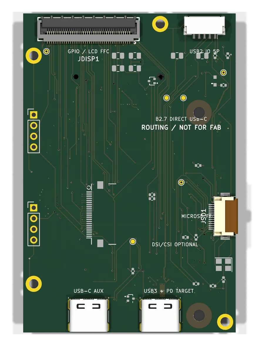
B2.7

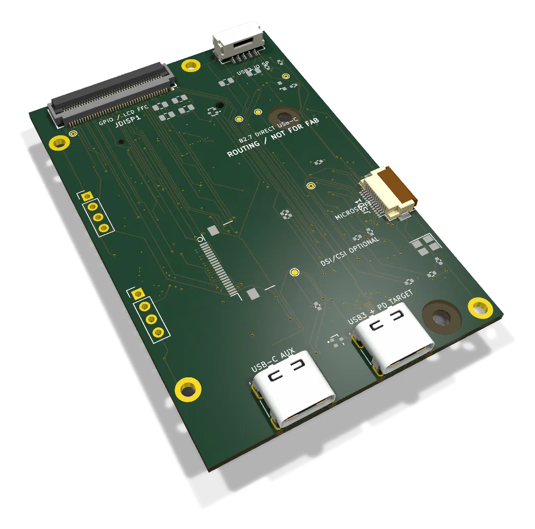
Direct USB-C fabrication routing

Fab gated · 6 opens B2 line · compact portrait

Restores the complete USB 3/Type-C front end on the compact 50.4 × 75.5 mm outline. Errors-only DRC reports zero violations with six unconnected items and no exclusions; uses fine vias that must be quoted as a six-layer fine-hole board.

Outline
50.4 × 75.5 mm
Layers
6 Cu
Footprints
75
Branch
main
Commit
c4b47aa
B2.7 perspective render
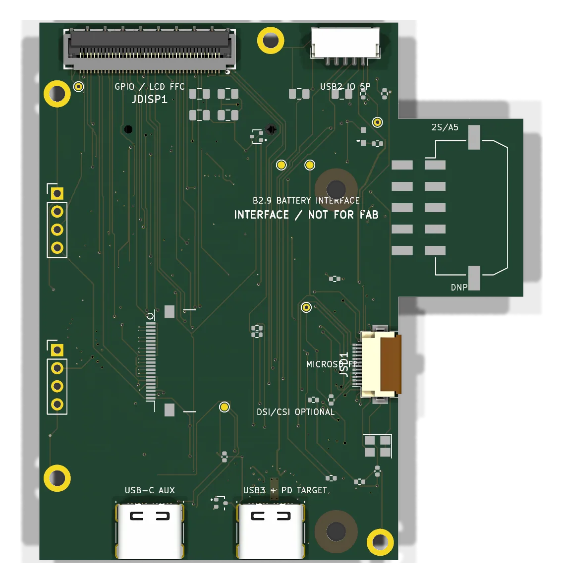
B2.9

Protected-2S battery interface

Interface checkpoint B2 line · compact portrait

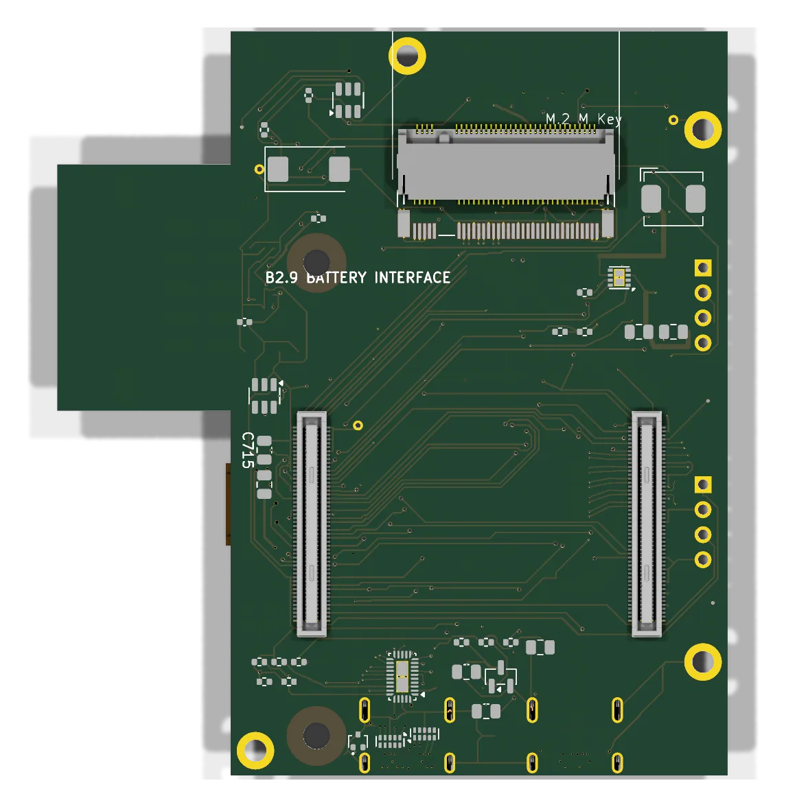
Interface and mechanical-placement checkpoint forked from B2.7 that adds one carrier battery connector on a local right-side wing between the USB 2.0 and microSD interfaces. The connector stays unpopulated until the charger and power path are settled.

Outline
68 × 75.5 mm
Layers
6 Cu
Footprints
76
Branch
codex/b2-9-battery-power
Commit
1c5e6f09d3
B2.9 perspective render
B2.8

HDMI, status LEDs and power switch

Fabrication blocked B2 line · compact portrait

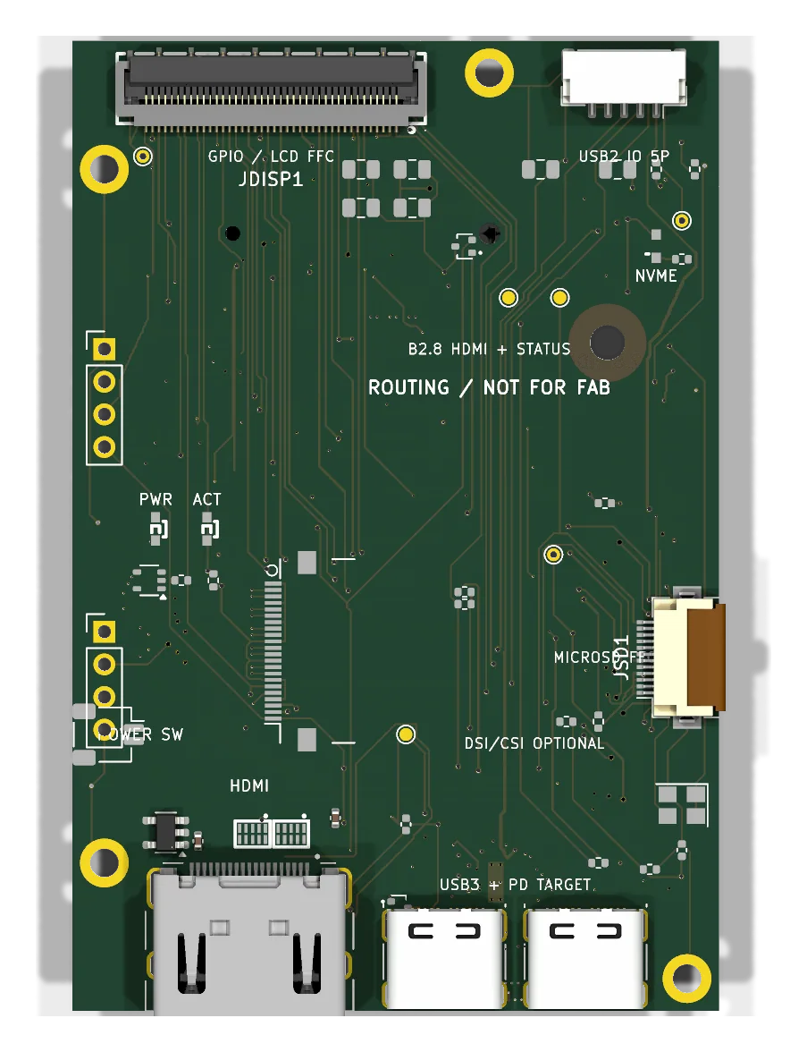
Forks B2.7 intact and adds a full-size HDMI receptacle on a lower-right wing, CM5IO-style power and activity indicators, and a keyed active-low power-switch input. Fabrication blocked until the schematic and routing complete.

Outline
50.4 × 75.5 mm
Layers
6 Cu
Footprints
88
Branch
main
Commit
0a5422e
B2.8 perspective render
B2.11

Top-side CM5 and Mini HDMI

Work in progress B2 line · compact portrait

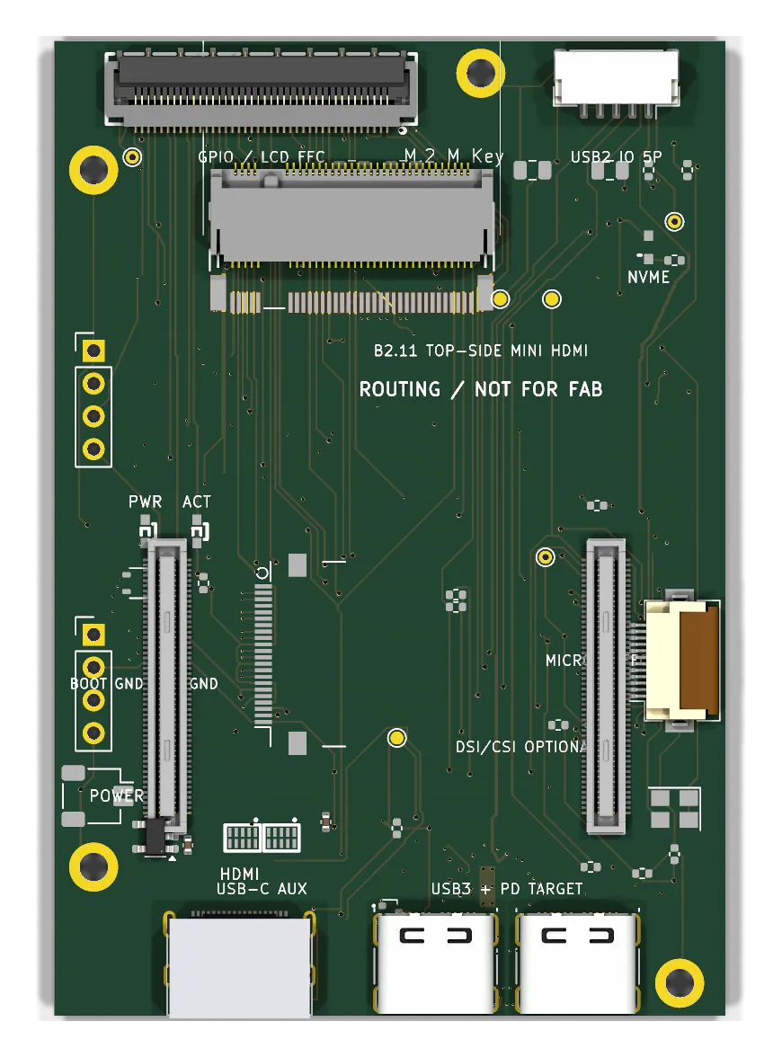
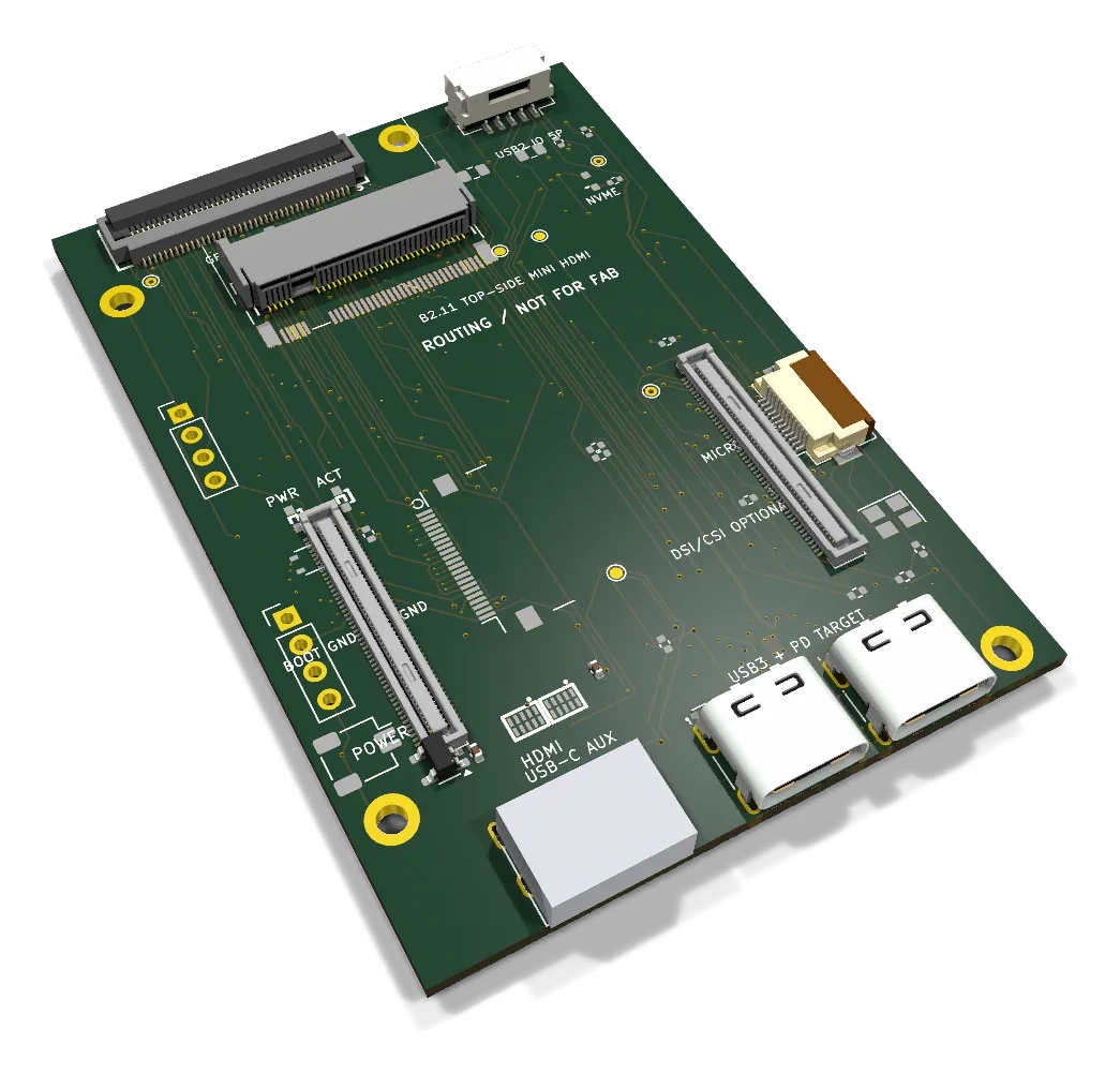
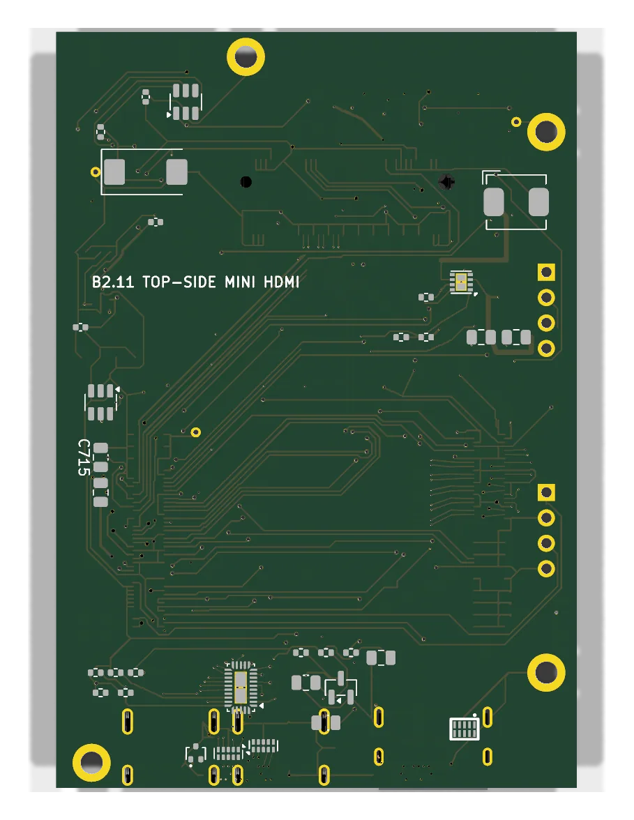
The short axis grows to a hard maximum of 52 mm while the CM5 sockets and the M.2 connector move to the top face and the edge HDMI receptacle becomes Mini HDMI. Adds the power-switch and boot/service landings that later revisions keep.

Outline
52 × 75.5 mm
Layers
6 Cu
Footprints
88
Branch
main
Commit
f0cb67b
B2.11 perspective render
B2.12

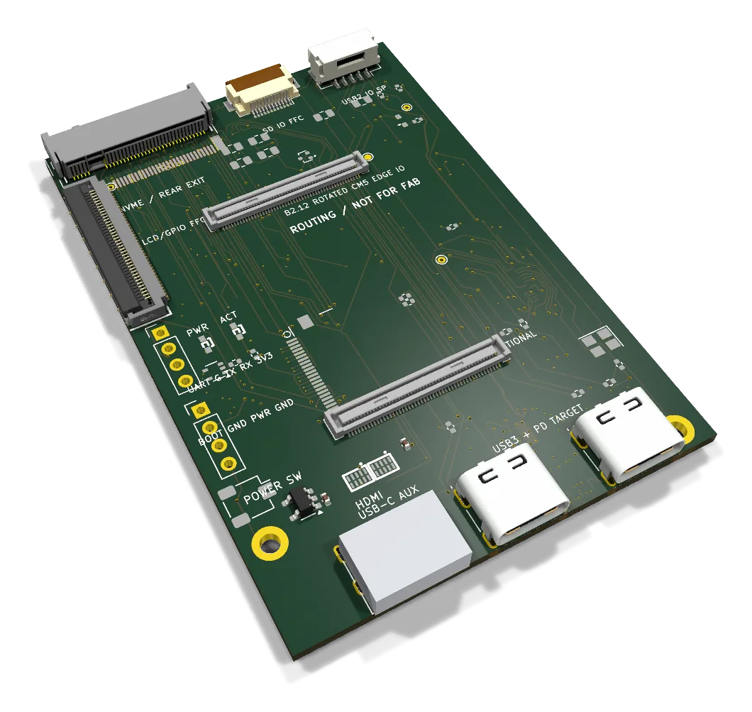
Rotated CM5, edge I/O

Placement reset B2 line · compact portrait

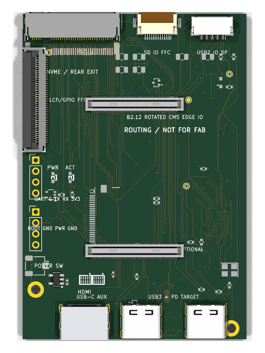
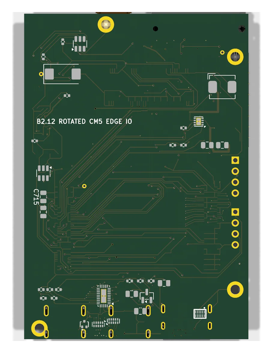
Placement and routing reset derived from B2.11 that rotates the CM5 arrangement and pushes the I/O to the board edges.

Outline
52 × 75.5 mm
Layers
6 Cu
Footprints
88
Branch
main
Commit
83f0bf1
B2.12 perspective render
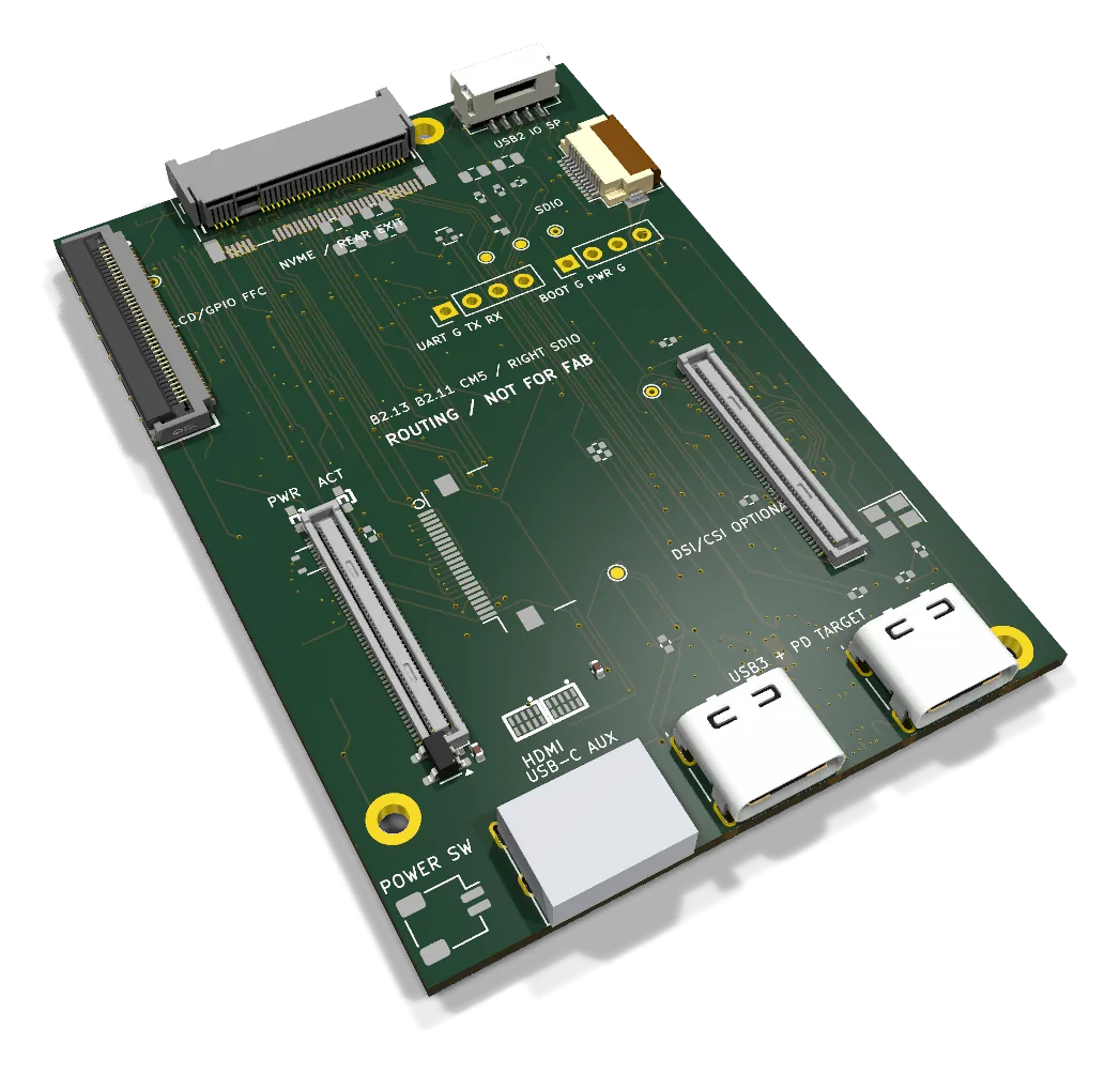
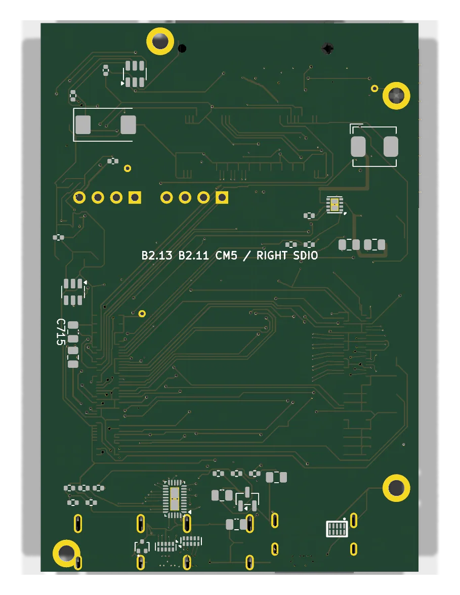
B2.13

CM5 right, SD I/O restored

Placement reset B2 line · compact portrait

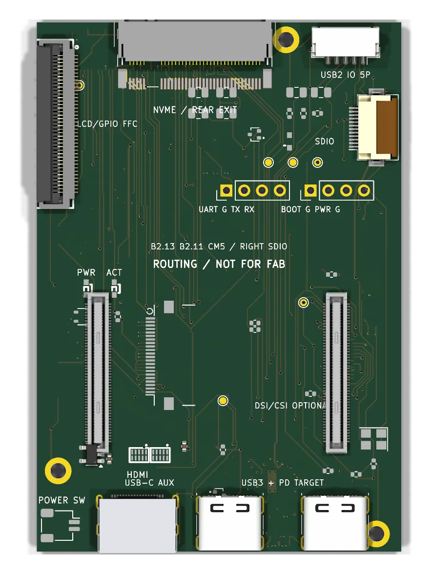
Placement and routing reset derived from B2.12 that restores the B2.11 CM5 position on the right and the SD I/O landing.

Outline
52 × 75.5 mm
Layers
6 Cu
Footprints
88
Branch
main
Commit
bfd5d8e
B2.13 perspective render
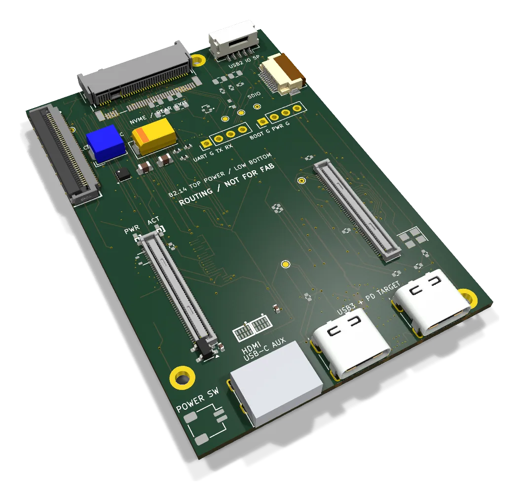
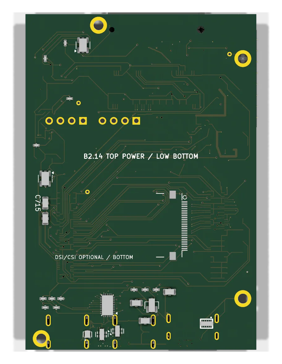
B2.14

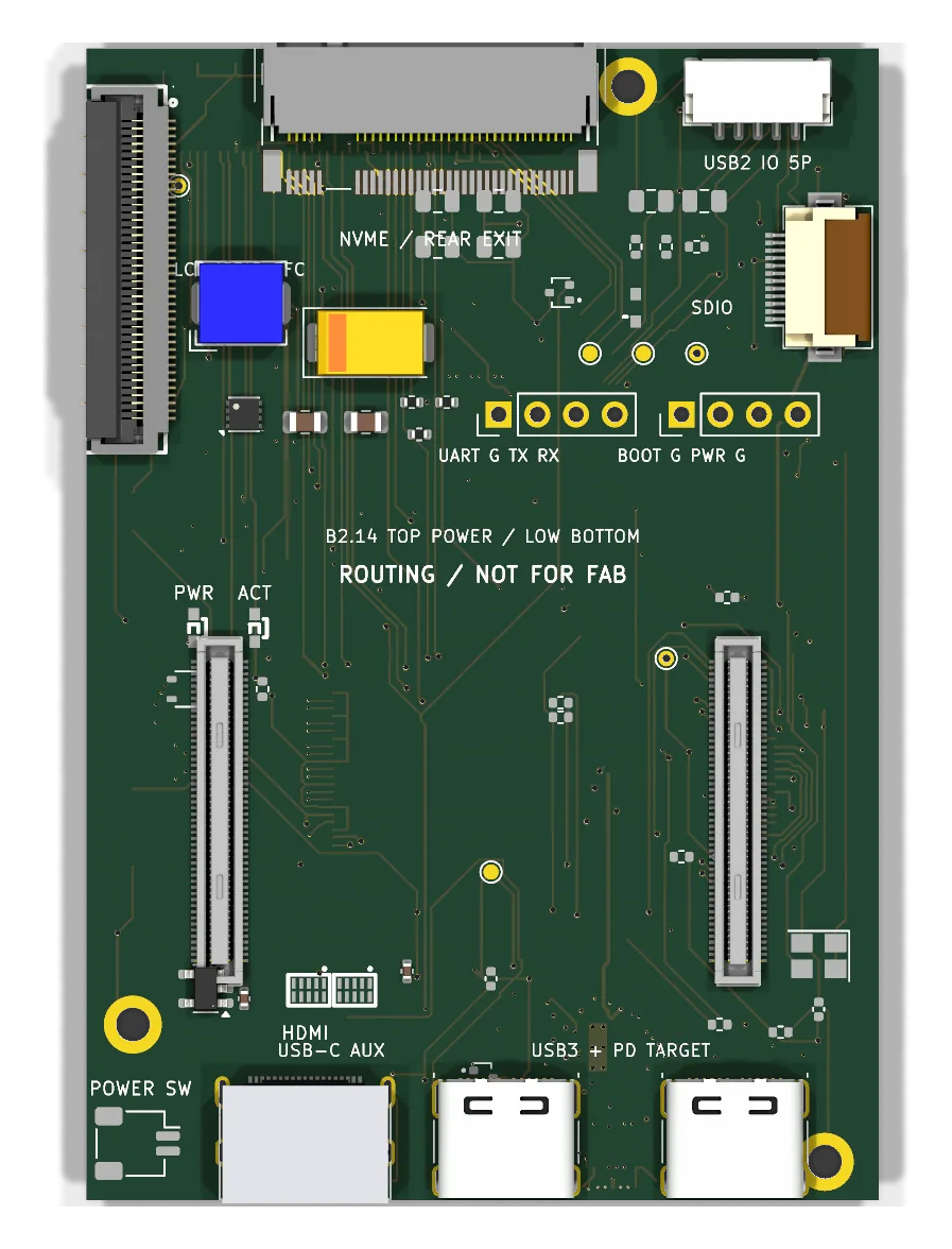
Bottom height reduction

Height reduction B2 line · compact portrait

Placement and routing reset that preserves the B2.13 interfaces while lowering the assembled bottom-side height.

Outline
52 × 75.5 mm
Layers
6 Cu
Footprints
88
Branch
main
Commit
a869043
B2.14 perspective render
B2.14.1

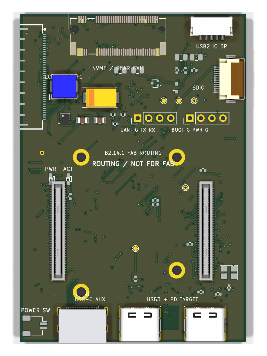
Fabrication routing checkpoint

Routing checkpoint B2 line · compact portrait

Reproducible routing checkpoint on the B2.14 floorplan.

Outline
52 × 75.5 mm
Layers
6 Cu
Footprints
88
Branch
main
Commit
e9efb14
B2.14.1 perspective render
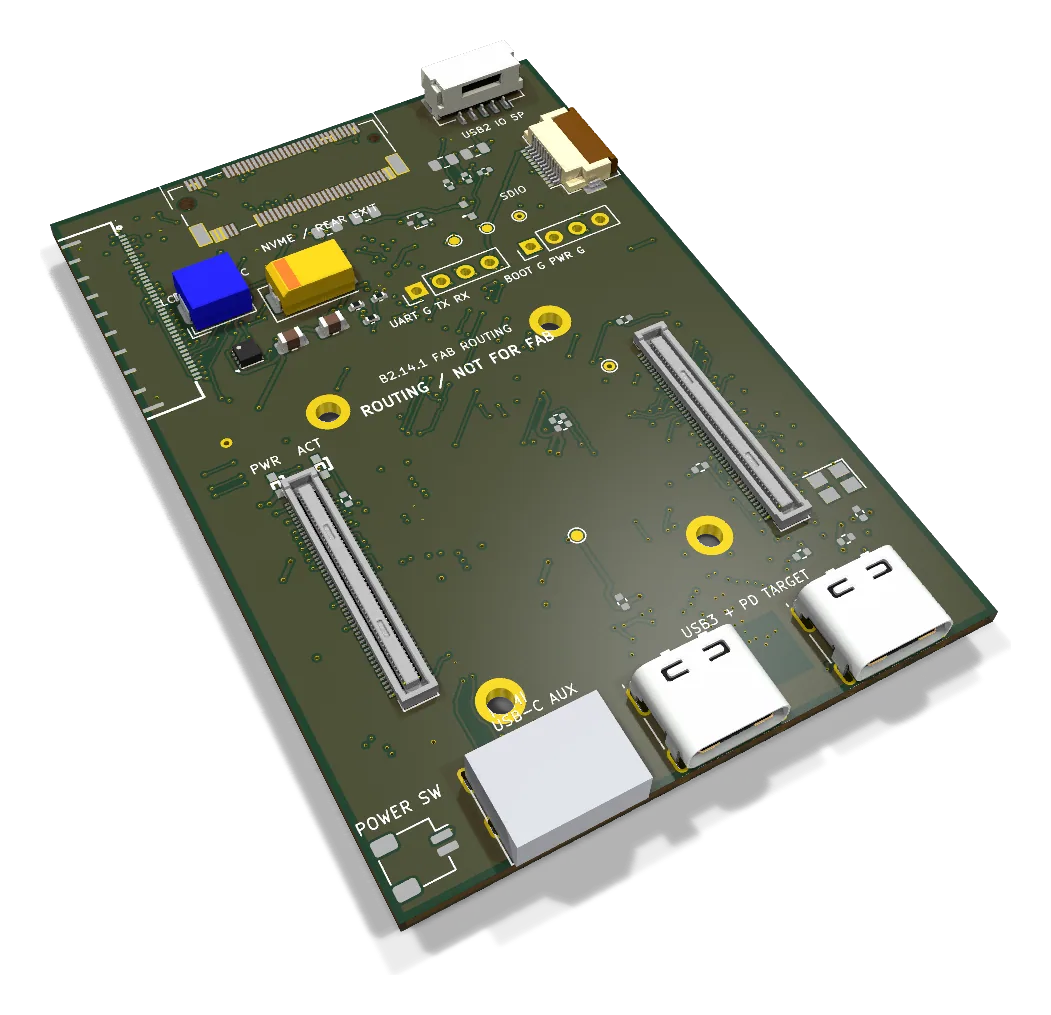
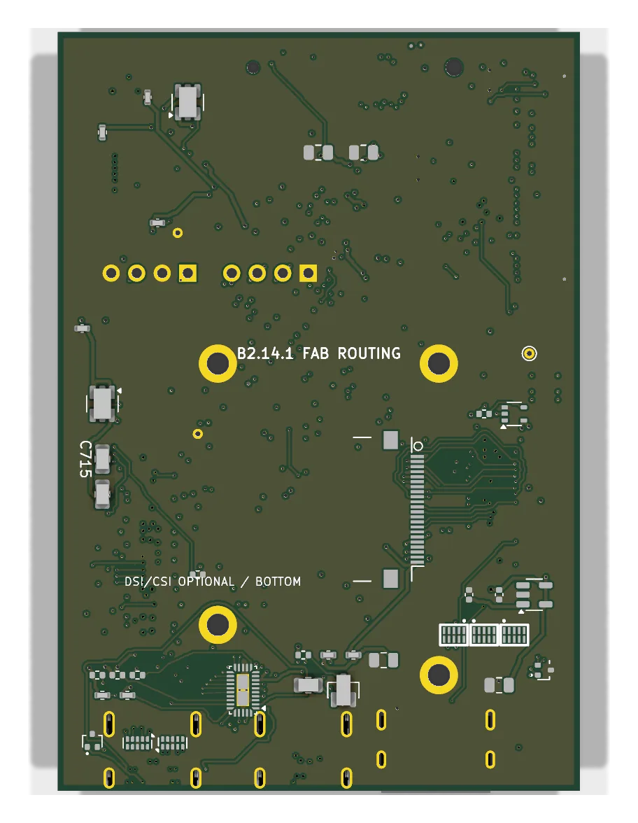
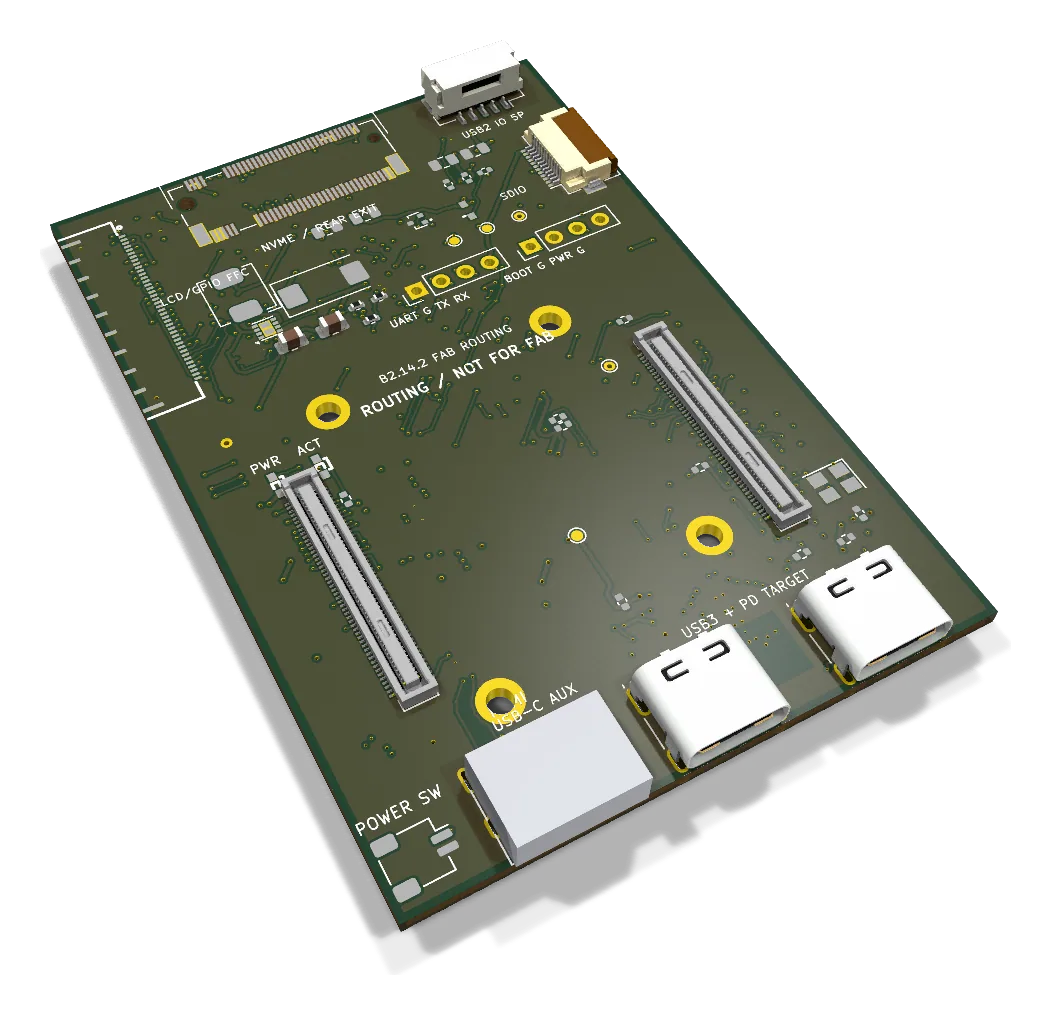
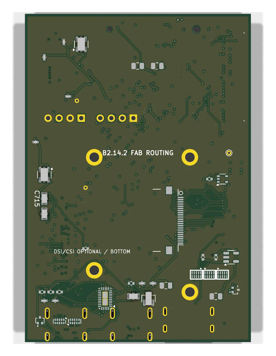
B2.14.2

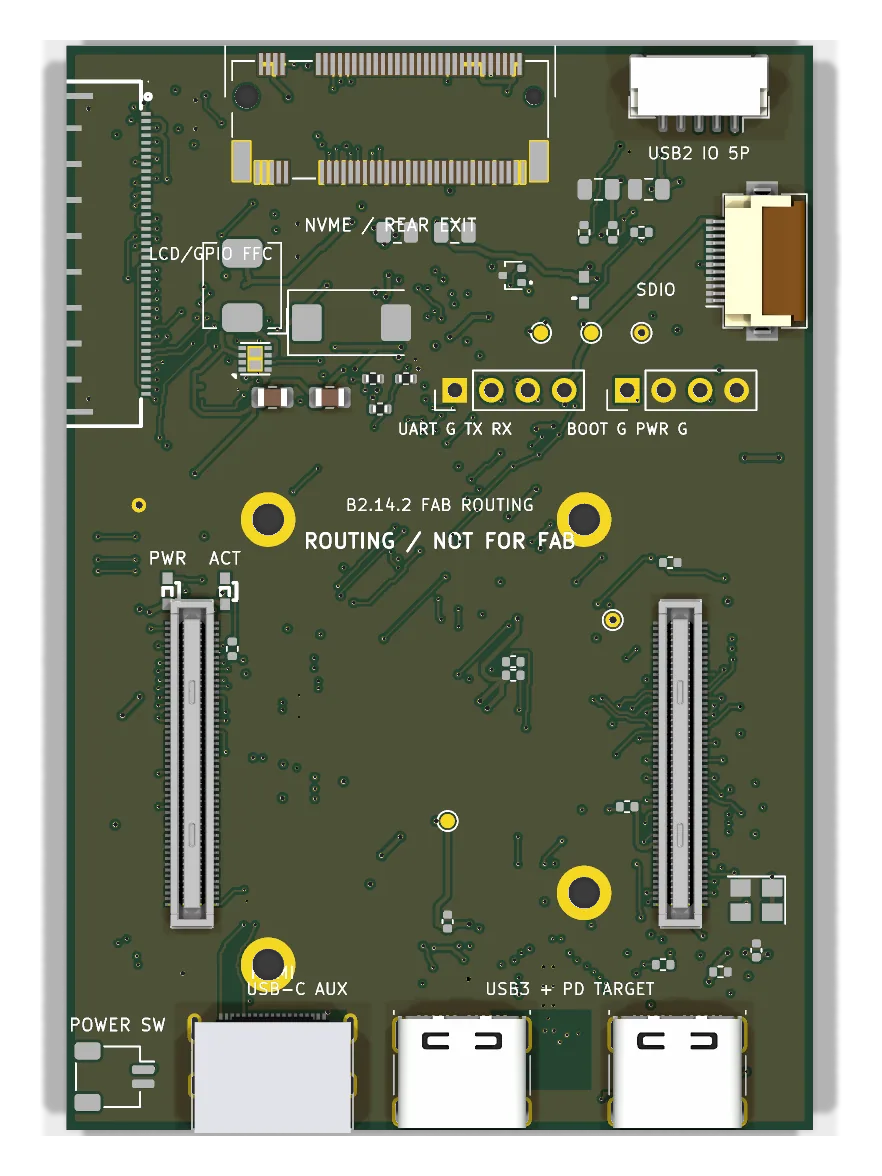
Routing and height review

Routing checkpoint B2 line · compact portrait

Forked from the reproducible B2.14.1 checkpoint. Its height review produced the flush-bottom decision that B2.15 implements.

Outline
52 × 75.5 mm
Layers
6 Cu
Footprints
88
Branch
main
Commit
061defd
B2.14.2 perspective render
B2.15

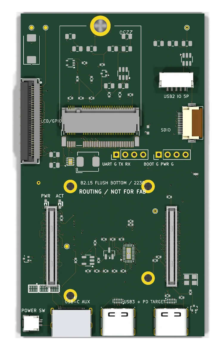
Flush bottom, onboard 2230

Mechanical decision · unrouted B2 line · compact portrait

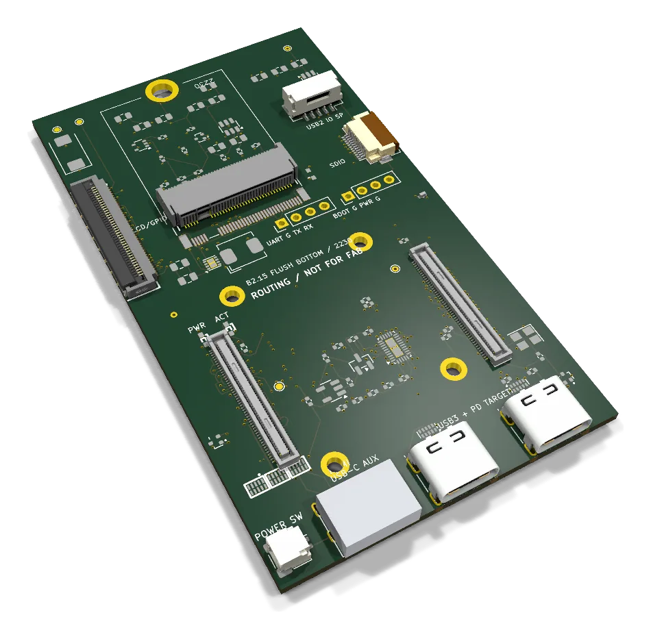
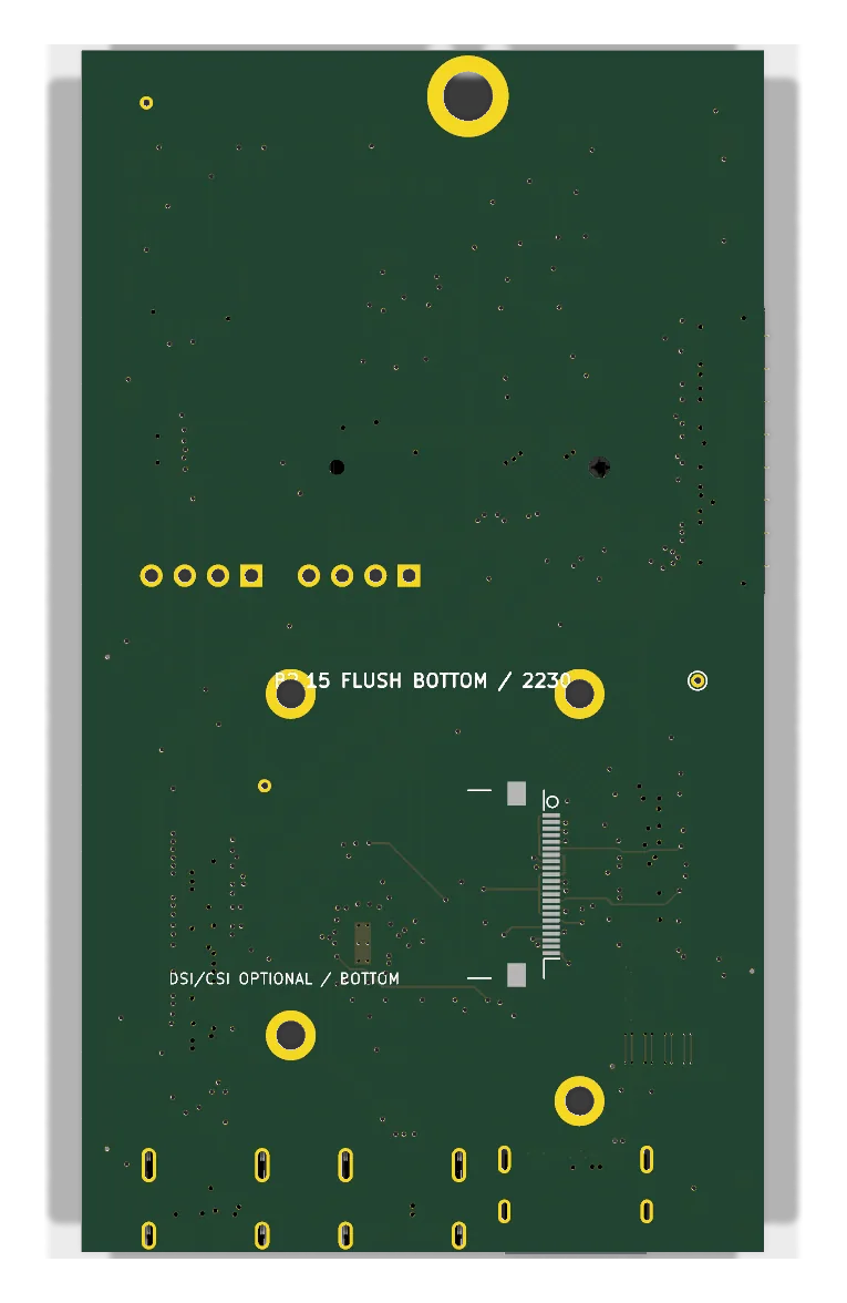
Keeps the short dimension at 52 mm and extends the long one to 91.5 mm so every fitted part sits on the top side and the assembled bottom has no height governor. Provides a flush plated retention hole for a 2230 drive; longer drives overhang the rear edge. The all-top placement invalidates the B2.14.2 routes.

Outline
52 × 91.5 mm
Layers
6 Cu
Footprints
89
Branch
main
Commit
6969671
B2.15 perspective render
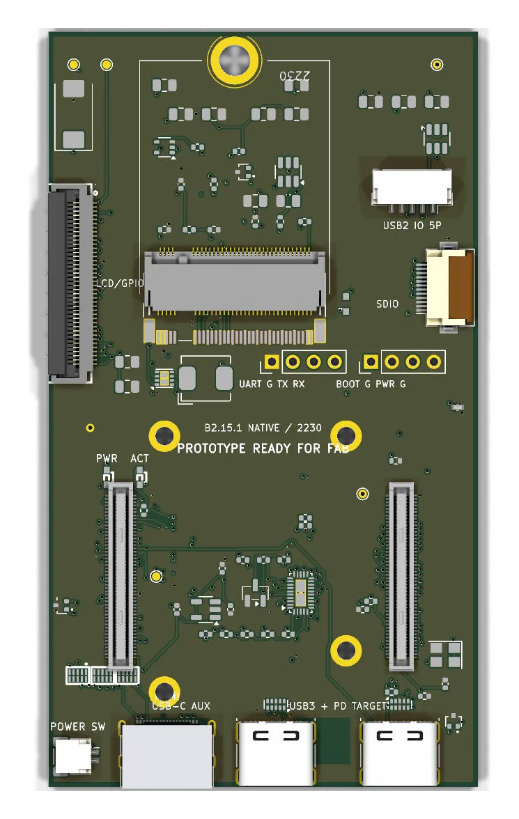
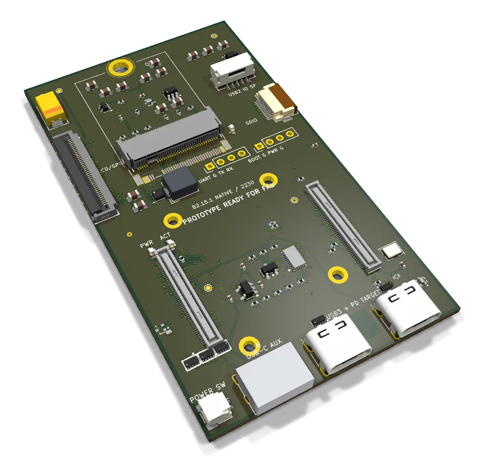
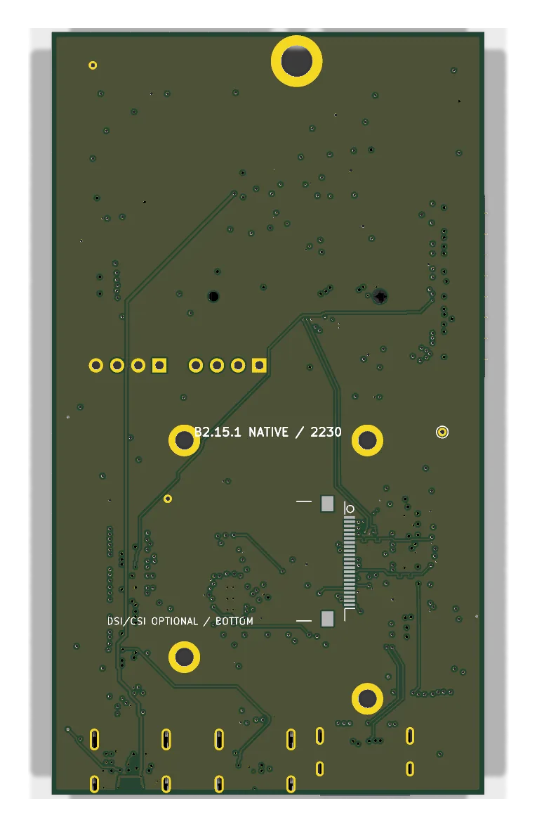
B2.15.1

Native reroute

Fabrication-ready routing B2 line · compact portrait

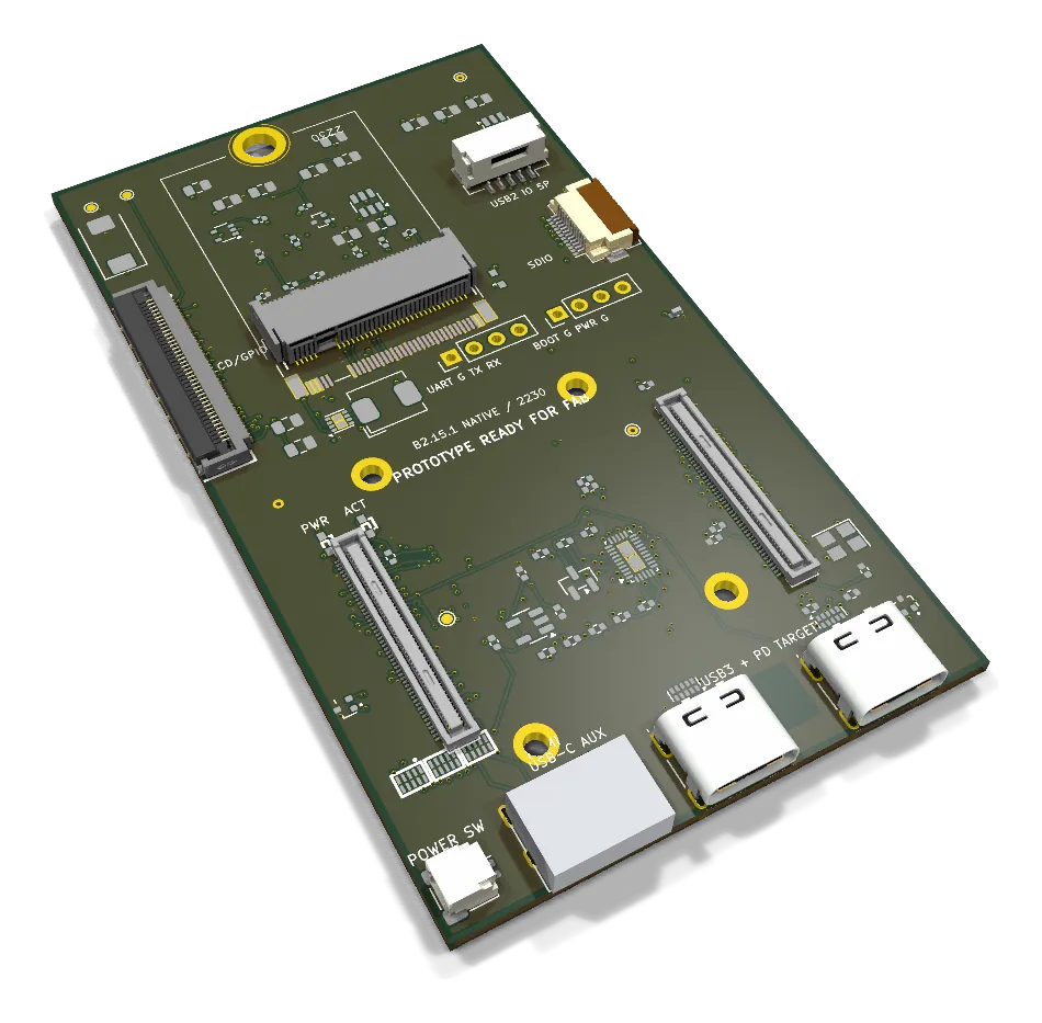
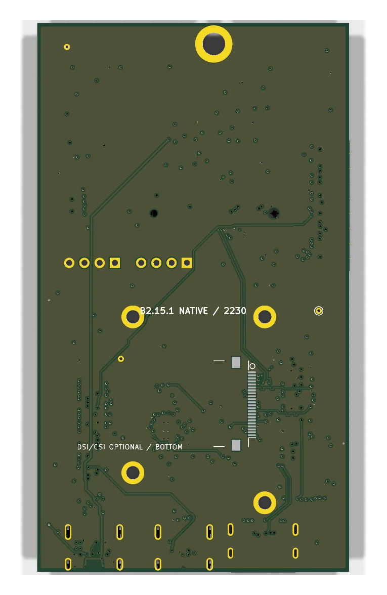
The fabrication successor to the B2.15 floorplan with a new native six-layer route.

Outline
52 × 91.5 mm
Layers
6 Cu
Footprints
89
Branch
main
Commit
8dc4ca0
B2.15.1 perspective render
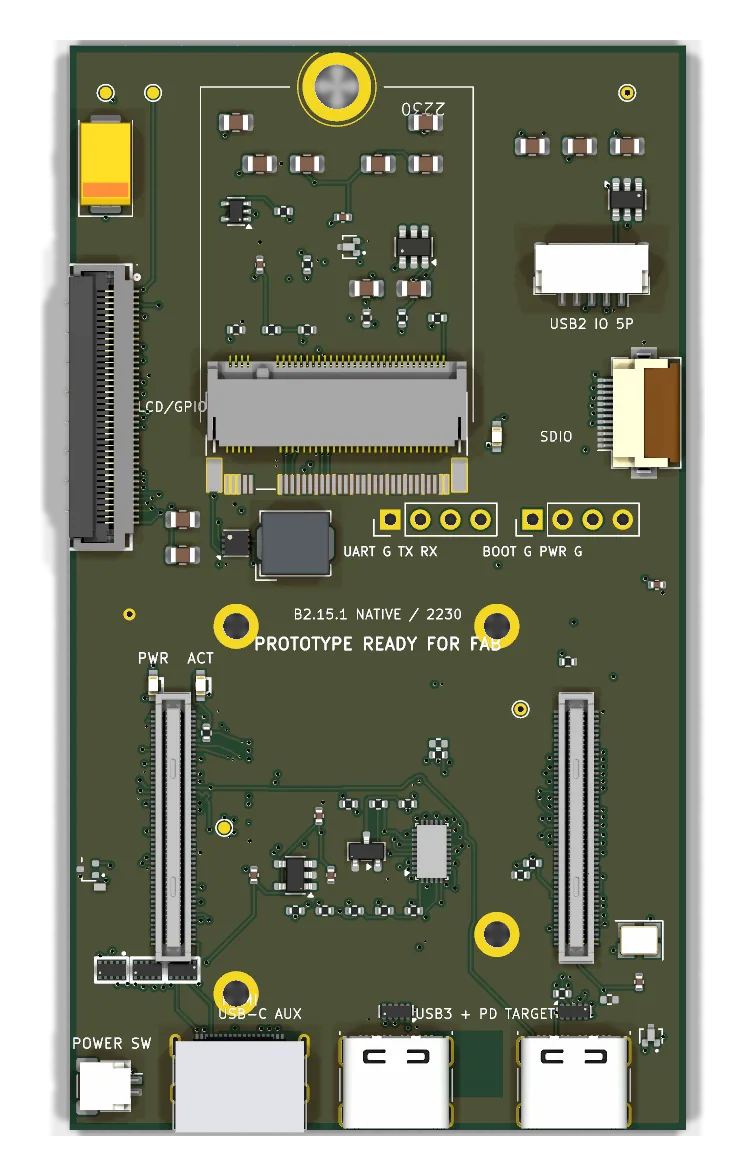
B2.15.2

Complete 3D model coverage

DRC clean baseline B2 line · compact portrait

Model-only fork of B2.15.1 with checked-in, reproducible 3D bodies for all 73 fitted components and no geometry change. Zero errors-only DRC violations, zero opens: the clean baseline that B2.17 later restarts from.

Outline
52 × 91.5 mm
Layers
6 Cu
Footprints
89
Branch
main
Commit
e725327
B2.15.2 perspective render
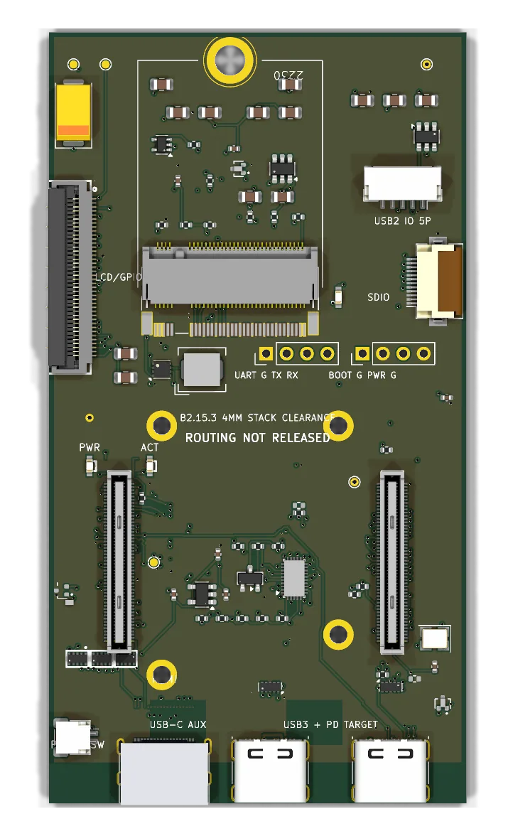
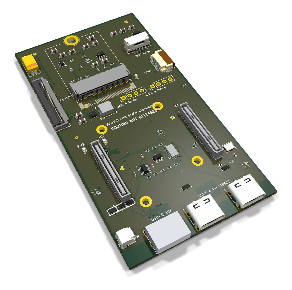
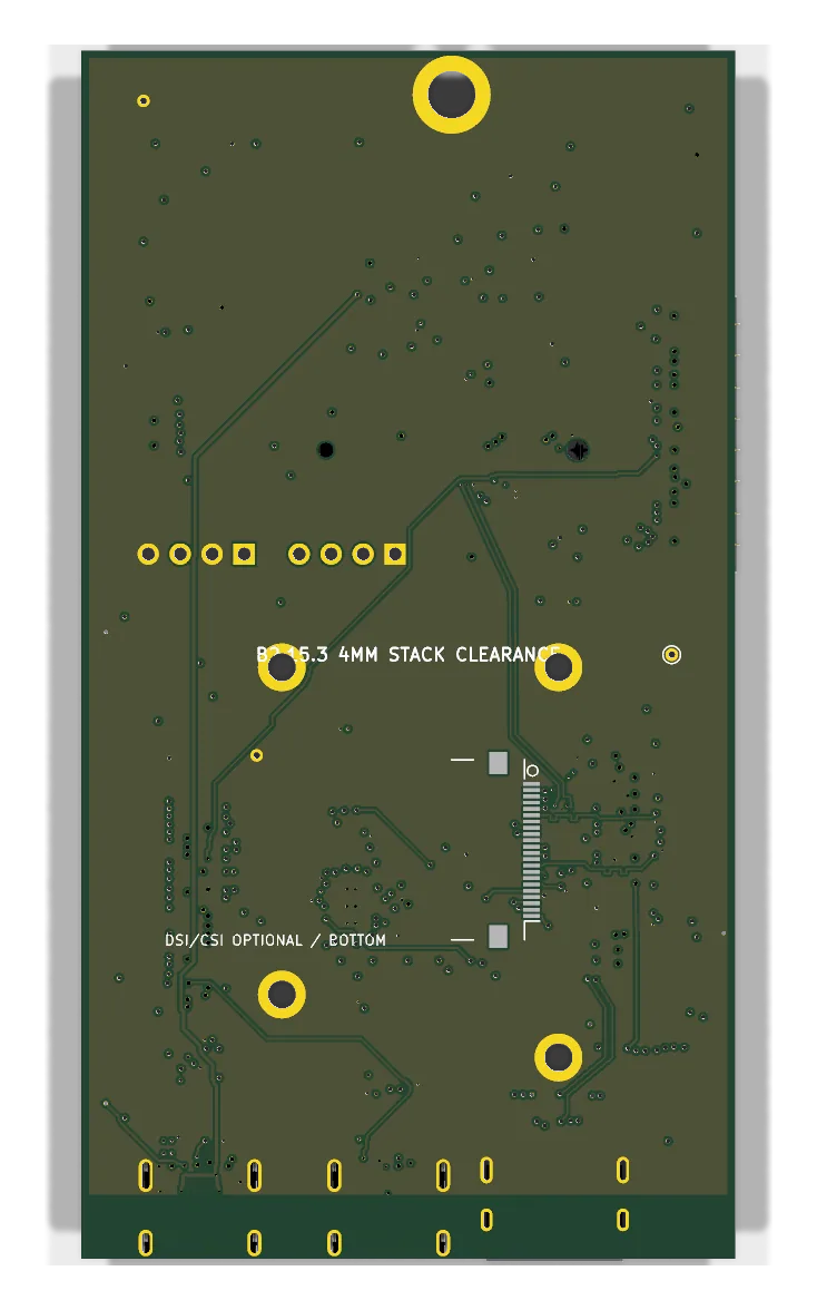
B2.15.3

CM5 clearance floorplan

Routing checkpoint · opens B2 line · compact portrait

Mechanically corrected successor to B2.15.2 that opens clearance around the CM5 sockets; a routing checkpoint whose front ports were left with opens.

Outline
52 × 96 mm
Layers
6 Cu
Footprints
89
Branch
main
Commit
852b819
B2.15.3 perspective render
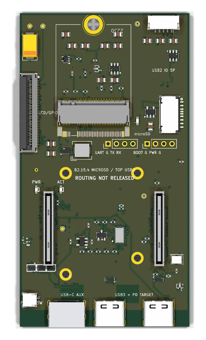
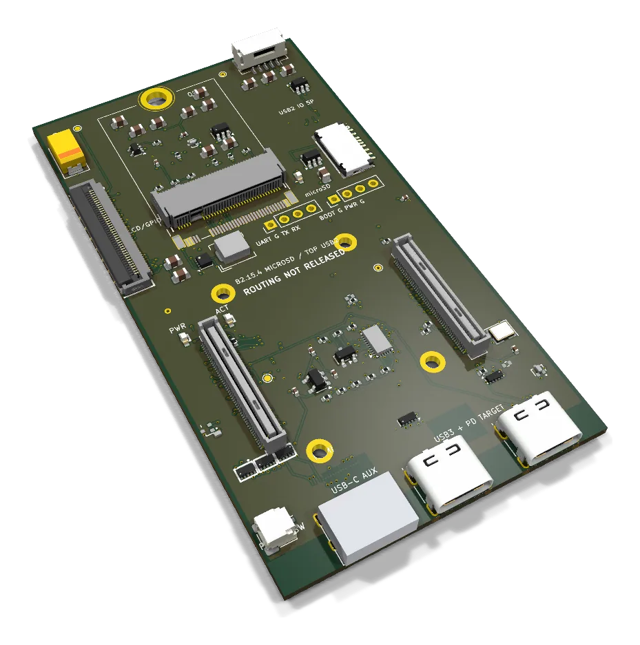
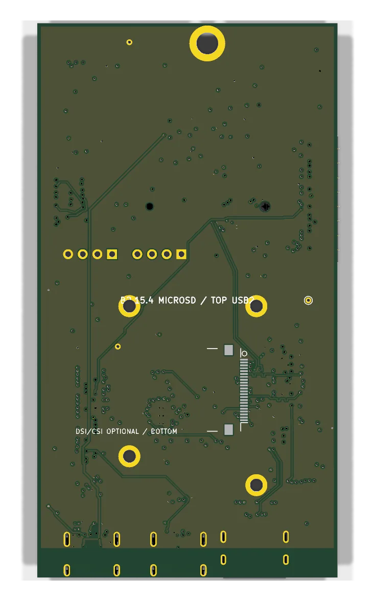
B2.15.4

microSD and top-edge USB 2.0

Routed prototype B2 line · compact portrait

Routed prototype successor that replaces the external microSD FFC with an onboard socket and moves USB 2.0 to the top edge.

Outline
52 × 96 mm
Layers
6 Cu
Footprints
91
Branch
main
Commit
8ea0916
B2.15.4 perspective render
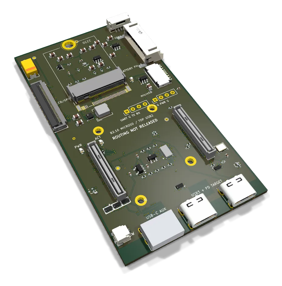
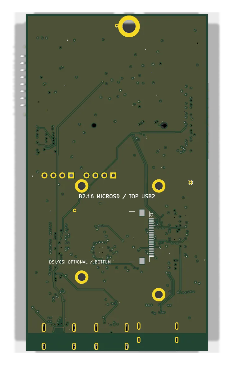
B2.16

JST PH-8 battery link

Electrically invalid B2 line · compact portrait

Adds the carrier half of a straight-through JST PH-8 link to the protected 2S pack controller on the right edge above microSD. Native DRC exposed 192 errors and 59 opens: the connector bodies fit but the copper did not, so the floorplan was re-applied on a clean baseline as B2.17.

Outline
52 × 96 mm
Layers
6 Cu
Footprints
92
Branch
main
Commit
d92f84e
B2.16 perspective render
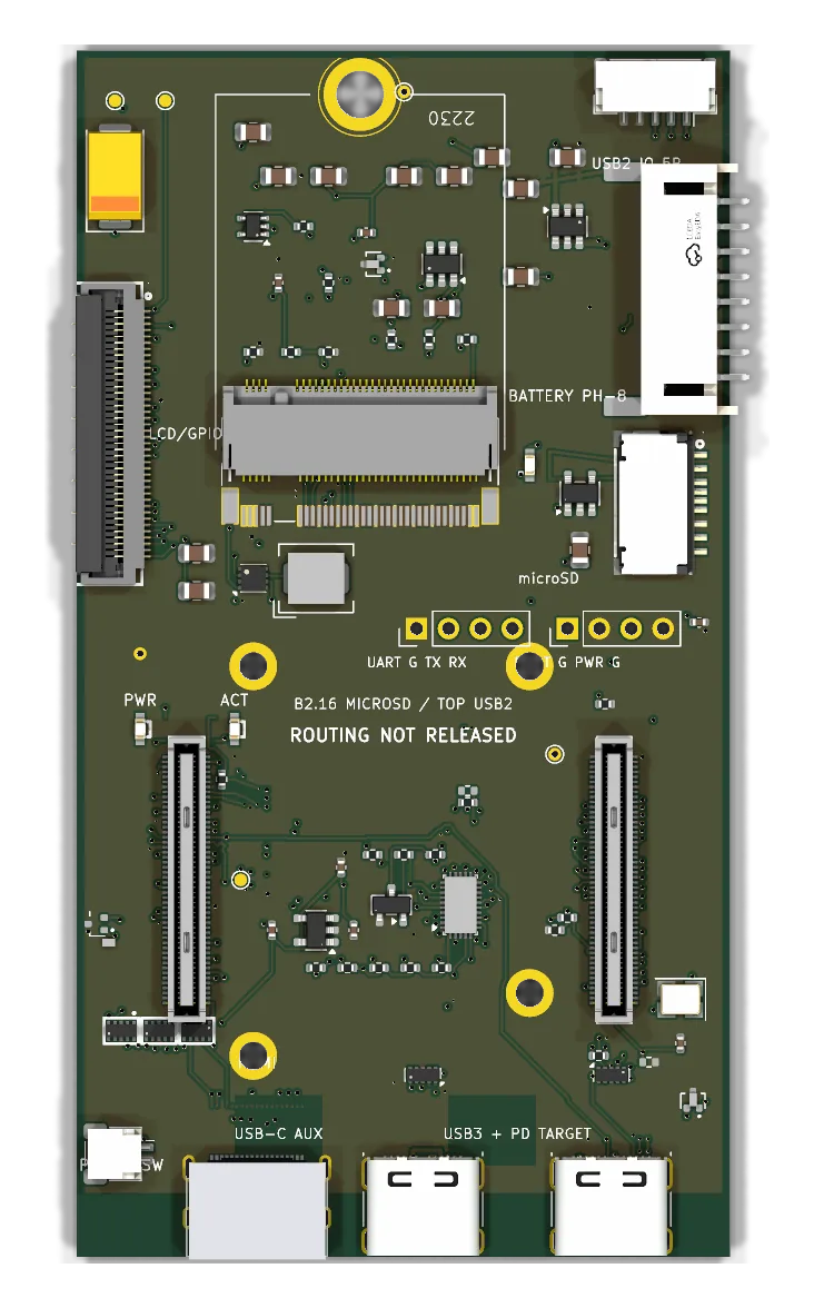
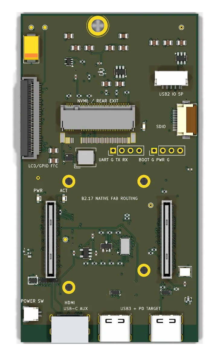
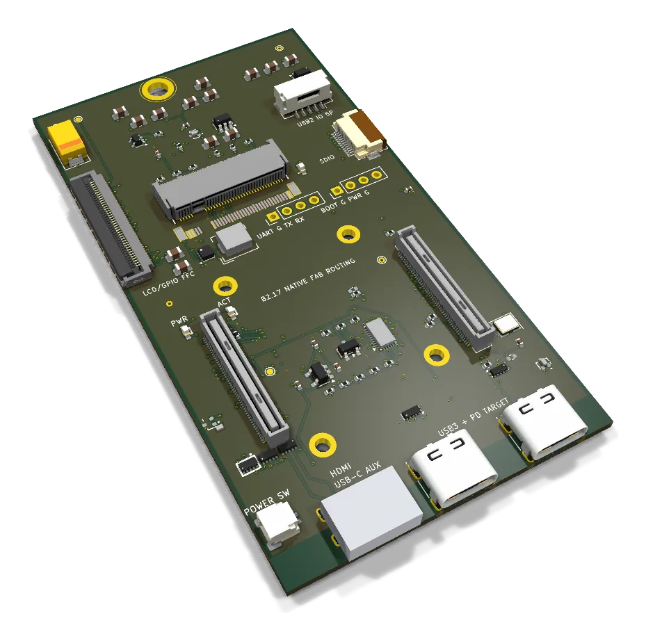
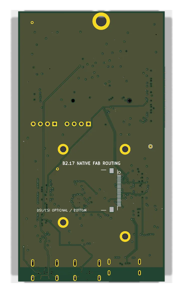
B2.17

Native fabrication-routing restart

Native routing checkpoint B2 line · compact portrait

Restarts from B2.15.2, the last source with zero DRC errors and zero opens, and re-applies the B2.16 floorplan one interface at a time with native DRC after each increment. Keeps the electrical baseline observable instead of letting a placement script certify its own routing.

Outline
52 × 96 mm
Layers
6 Cu
Footprints
89
Branch
main
Commit
93c0f88
B2.17 perspective render
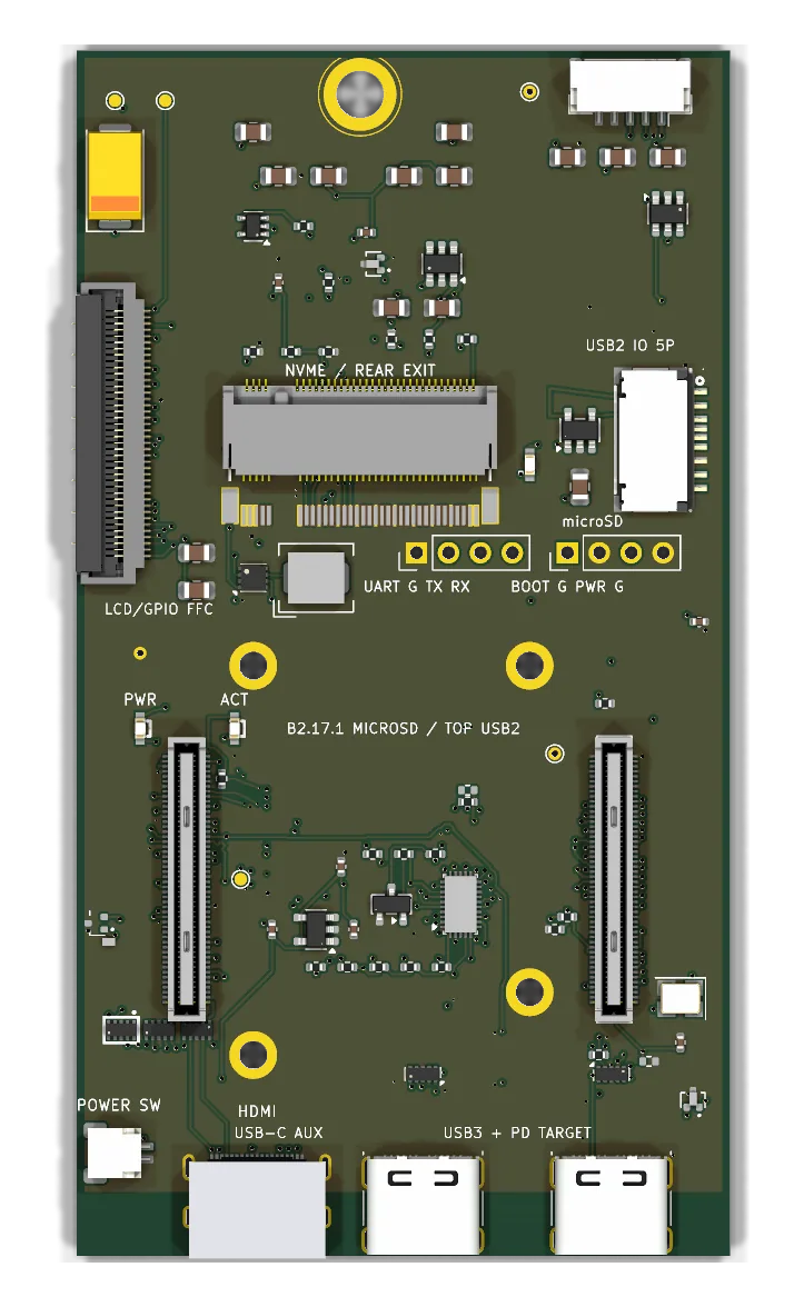
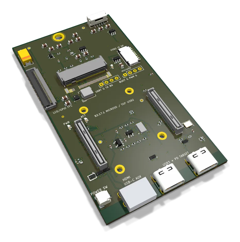
B2.17.1

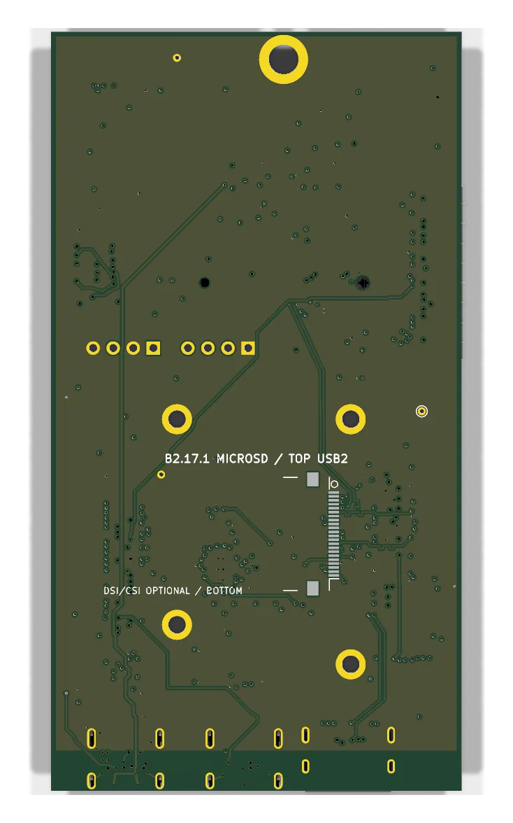
microSD top-edge USB 2.0 candidate

Candidate B2 line · compact portrait

The clean, charger-free successor to B2.17 with the microSD socket and top-edge USB 2.0 connector in their final positions.

Outline
52 × 96 mm
Layers
6 Cu
Footprints
91
Branch
main
Commit
d467b0d
B2.17.1 perspective render
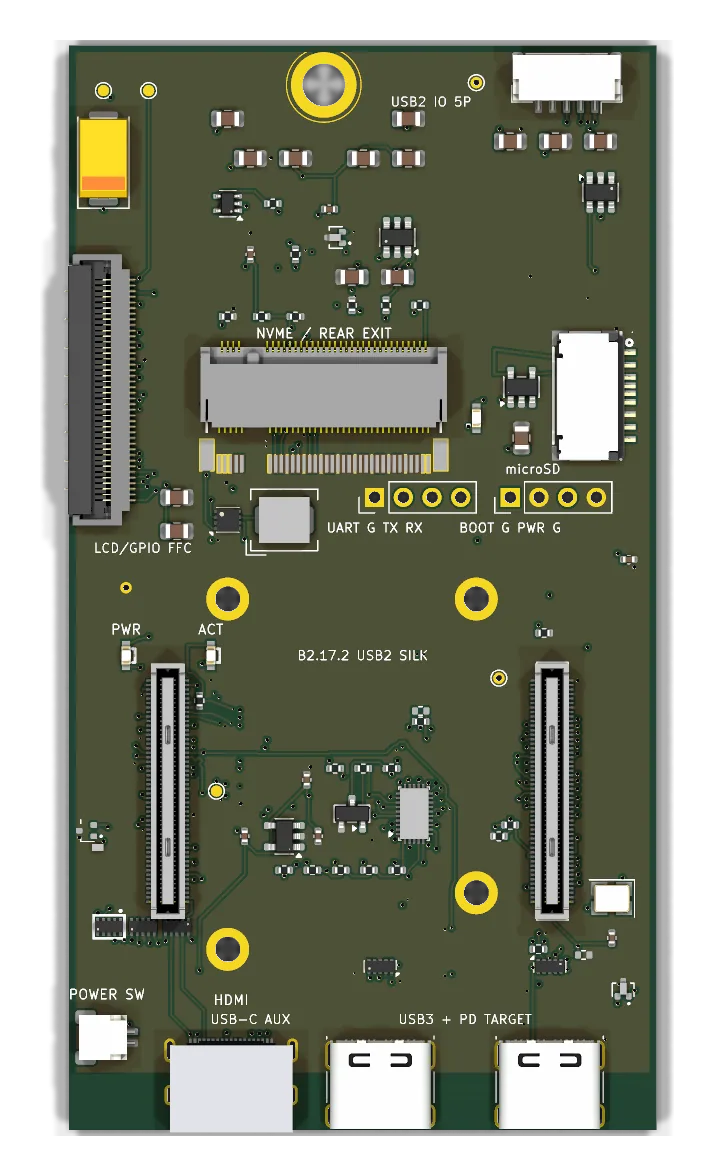
B2.17.2

Service silkscreen

Silkscreen only B2 line · compact portrait

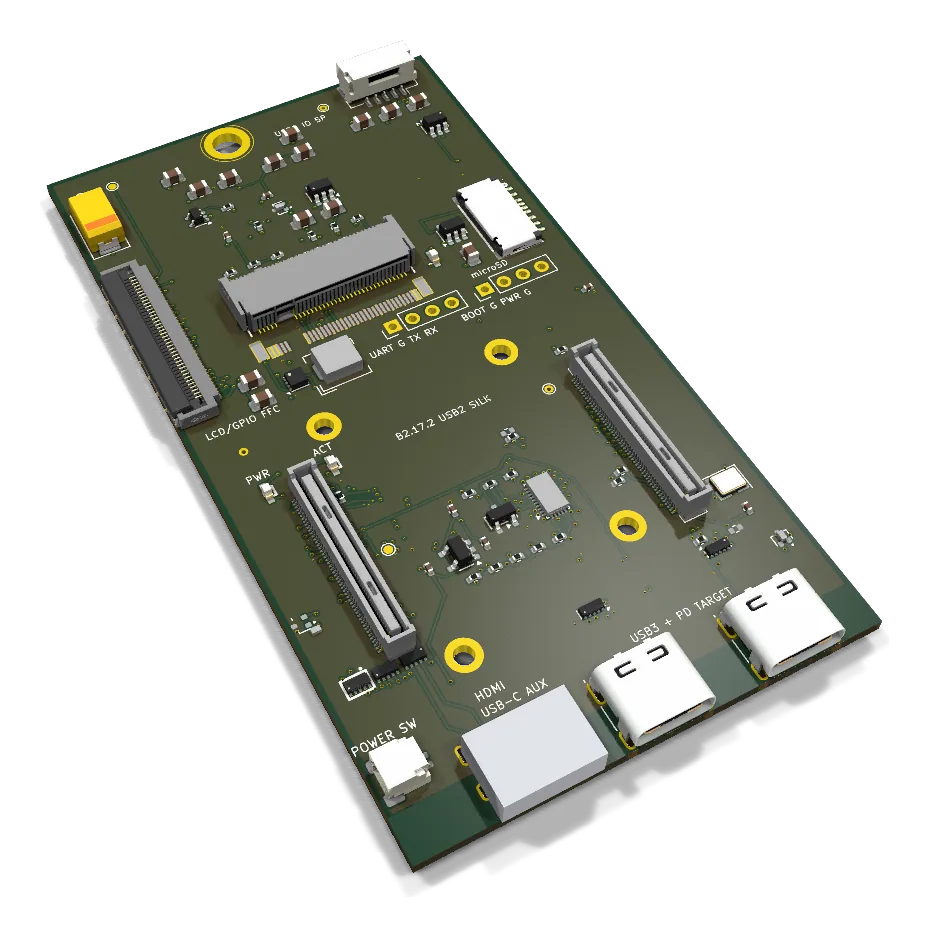
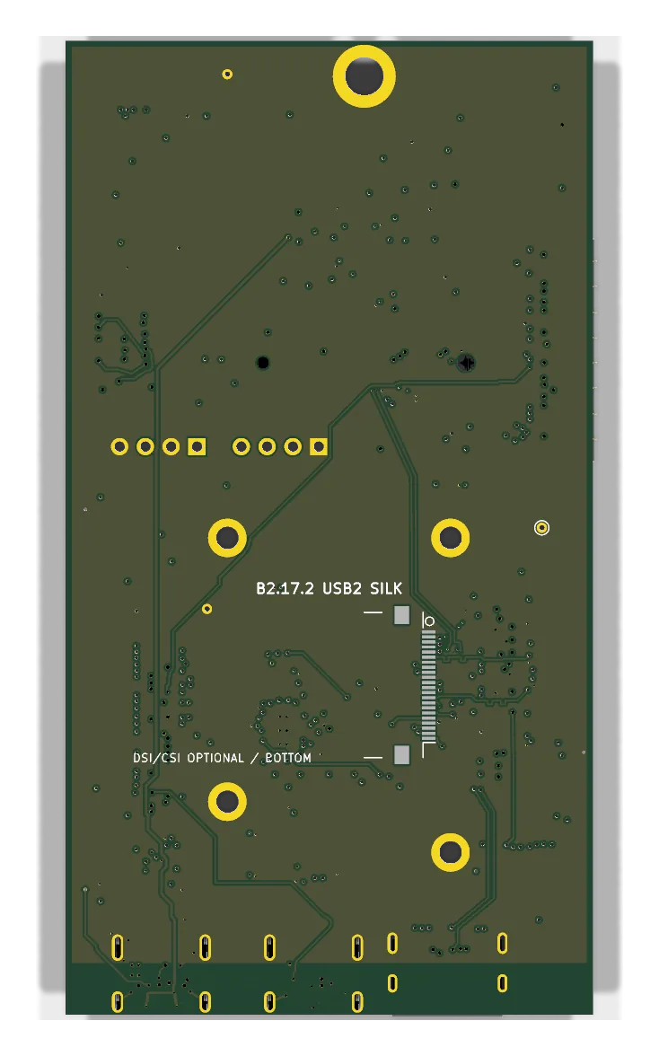
Silkscreen-only successor that labels the service landings and cleans up the USB 2.0 legend. No copper change.

Outline
52 × 96 mm
Layers
6 Cu
Footprints
91
Branch
main
Commit
c70a076
B2.17.2 perspective render
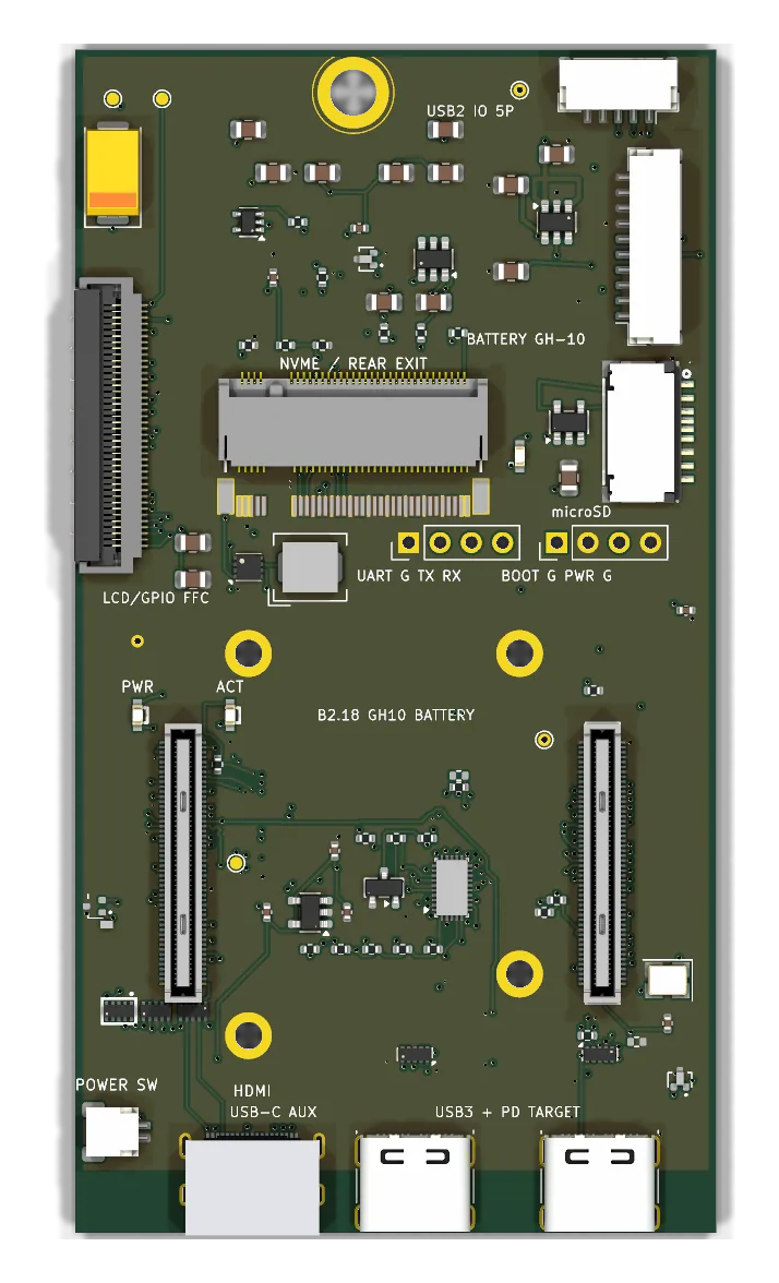
B2.18

GH-10 battery-link prototype

Battery-link prototype B2 line · compact portrait

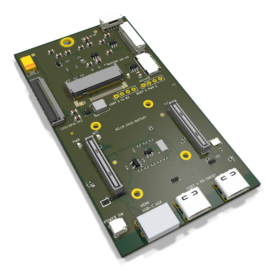
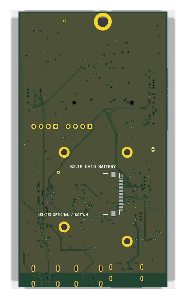
Proves that a 10-position side-entry JST GH battery connector fits between the USB 2.0 and microSD interfaces without growing the outline, electrically routed and passing errors-only DRC, ERC and parity checks. No fabrication files generated.

Outline
52 × 96 mm
Layers
6 Cu
Footprints
92
Branch
main
Commit
1f9c020
B2.18 perspective render
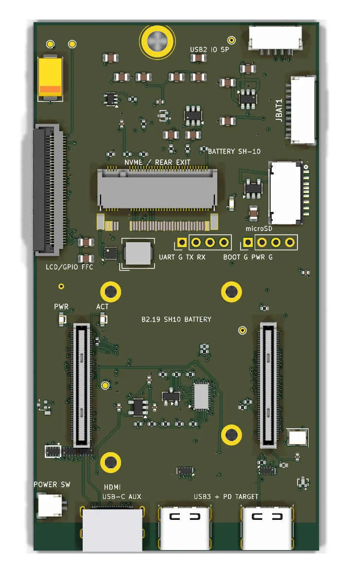
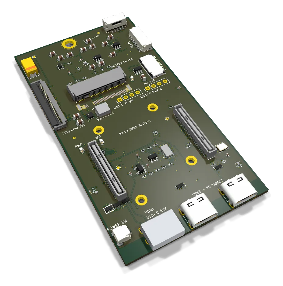
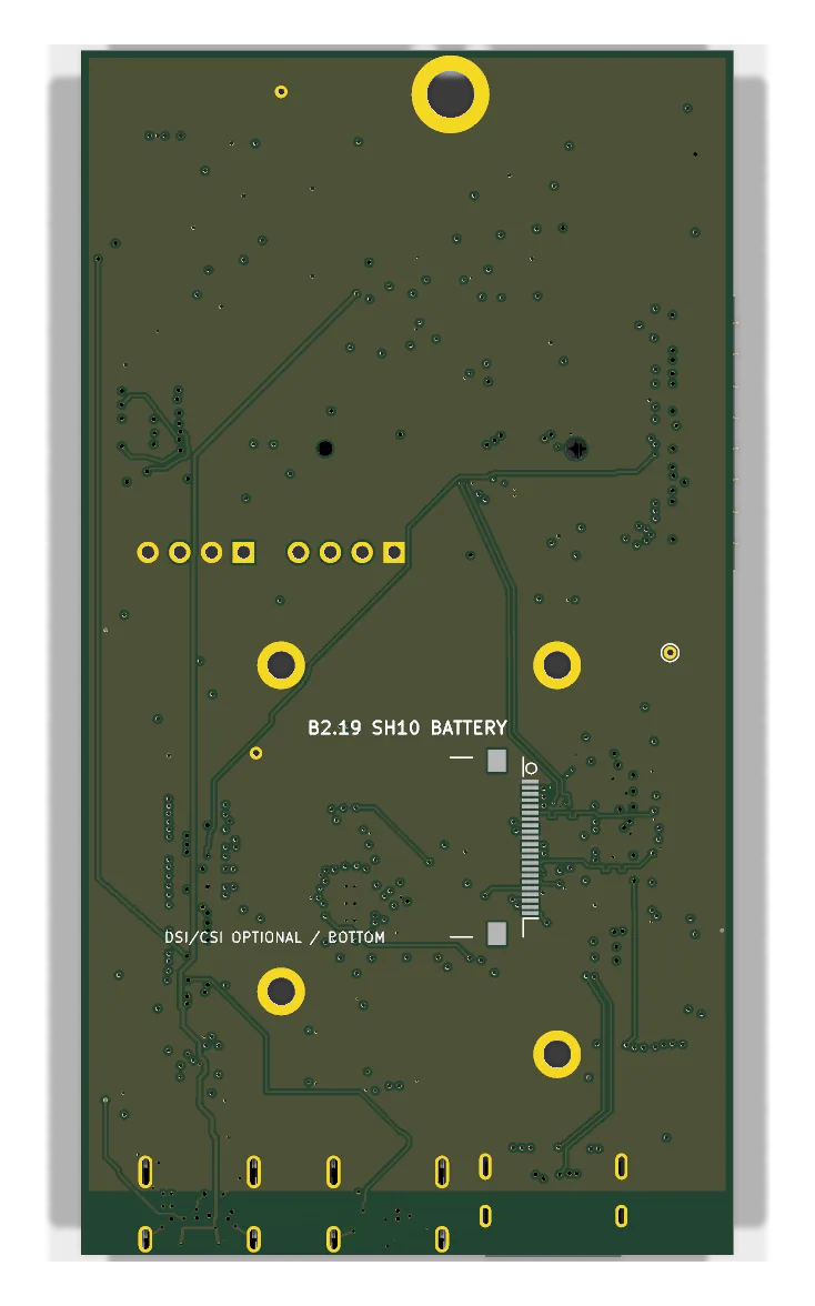
B2.19

SH-10 battery link

Released and quoted B2 line · compact portrait

Replaces B2.18's unavailable GH-10 with a stocked JST SH-10 connector and cable. Released and quoted with a fail-closed release builder.

Outline
52 × 96 mm
Layers
6 Cu
Footprints
92
Branch
main
Commit
f7c59cb
B2.19 perspective render

From B2.18

Continues as B2.20

Notes SH-10 batteryCable procurement and continuity
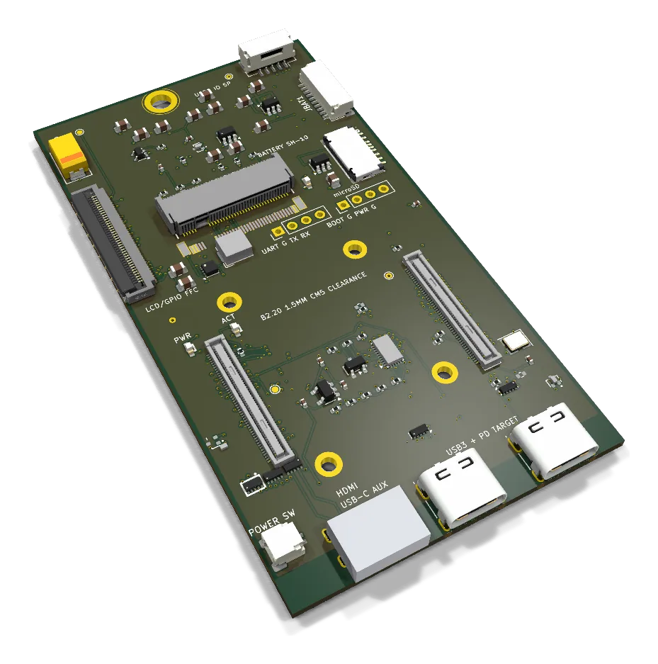
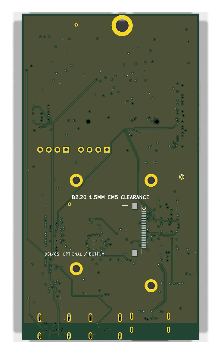
B2.20

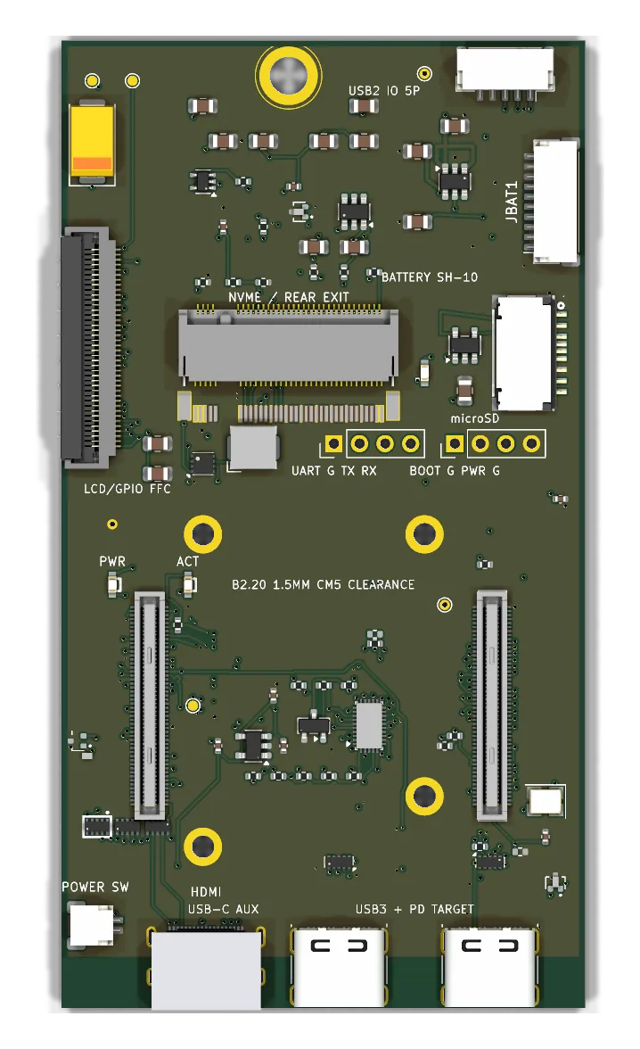
1.5 mm CM5 socket clearance

Electrically closed · quoted B2 line · compact portrait

Corrects a coupled mechanical and electrical problem in the CM5 socket stack and the clearance to a nearby inductor, moving to exact 1.5 mm Amphenol sockets. Electrically closed with zero errors and zero opens, then quoted.

Outline
52 × 96 mm
Layers
6 Cu
Footprints
92
Branch
main
Commit
e4b8b18
B2.20 perspective render

From B2.19

Continues as B2.21

Notes Socket clearance correctionB2.20 quote
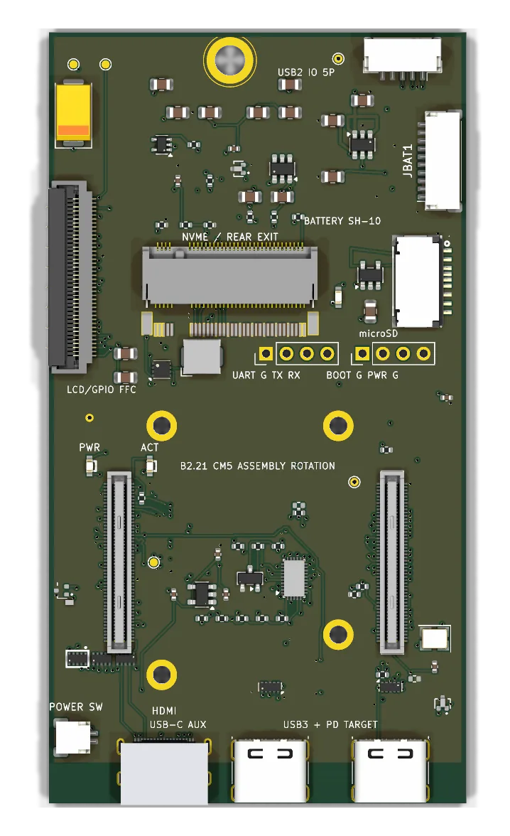
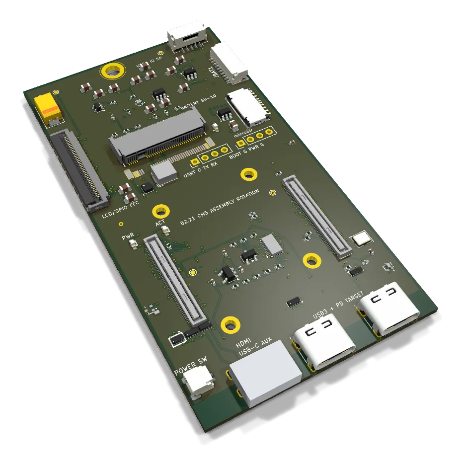
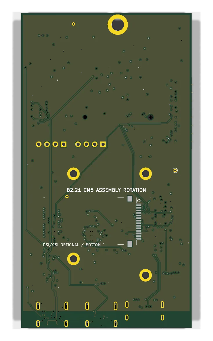
B2.21

CM5 assembly-rotation correction

Placement fix · vias rejected B2 line · compact portrait

Keeps the B2.20 geometry unchanged and fixes the assembler placement rotation for both CM5 sockets from 0° to 90°, with a fail-closed gate that checks pad geometry, STEP identity and the final placement rows together. The board house then rejected its blind and micro vias.

Outline
52 × 96 mm
Layers
6 Cu
Footprints
92
Branch
main
Commit
a344d04
B2.21 perspective render
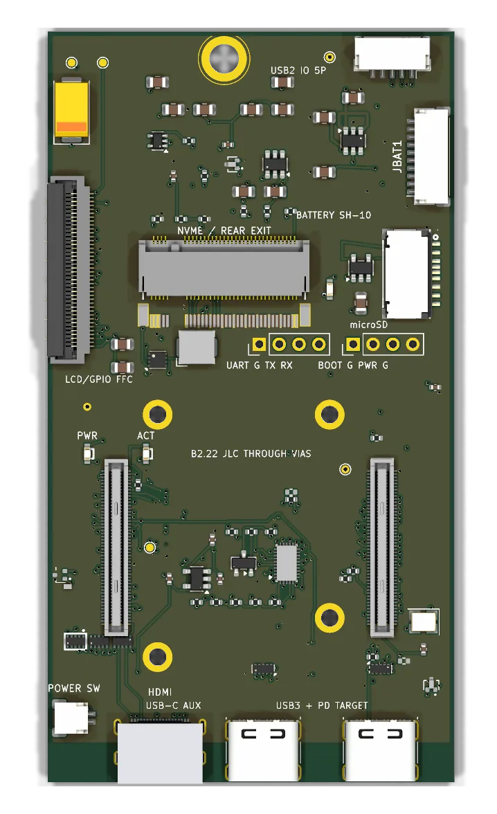
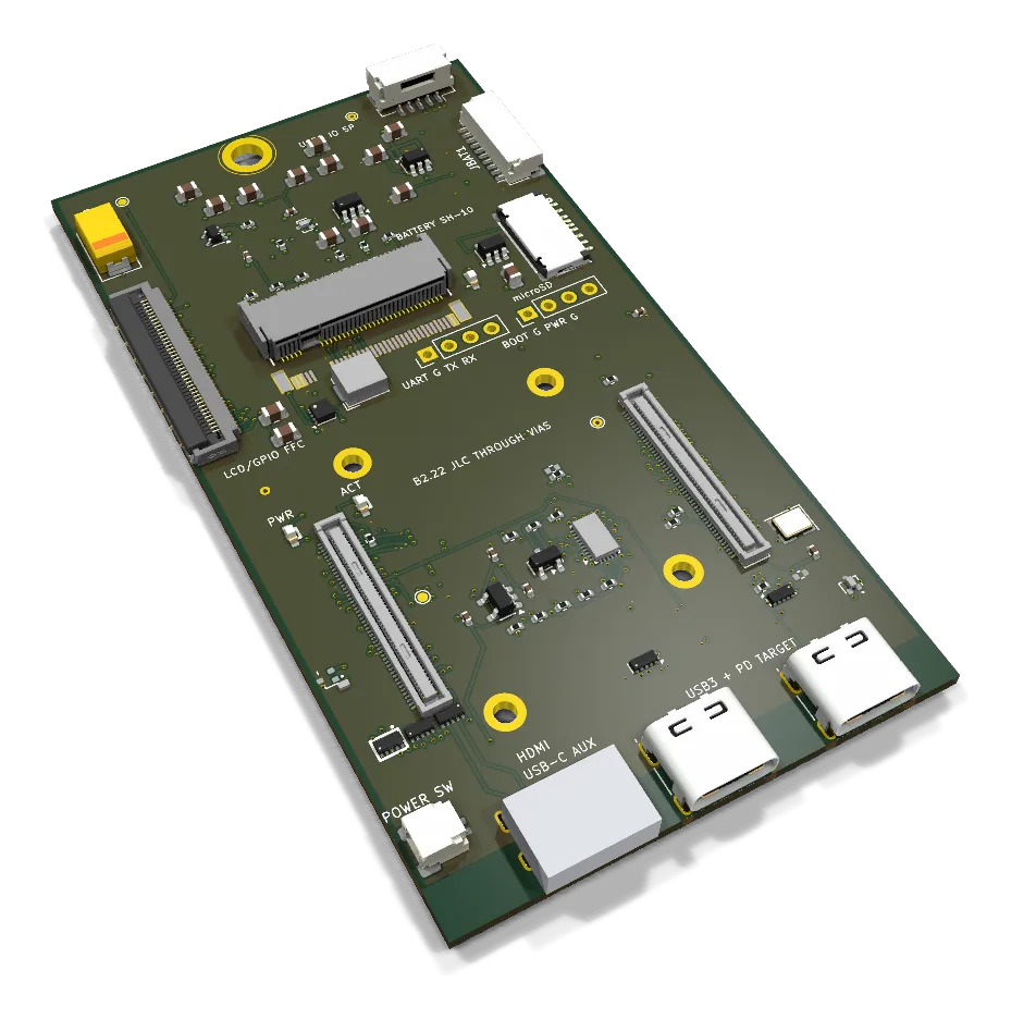
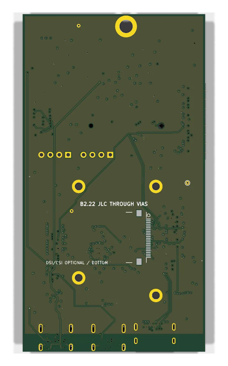
B2.22

Through-via correction

Released B2 line · compact portrait

Replaces the 22 microvias and 14 blind vias that the board house rejected with 36 ordinary plated through-vias. Circuit, placements, outline and population are unchanged; released to main.

Outline
52 × 96 mm
Layers
6 Cu
Footprints
92
Branch
main
Commit
0169447806
B2.22 perspective render
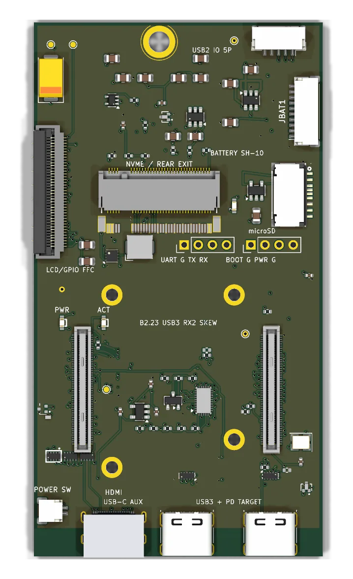
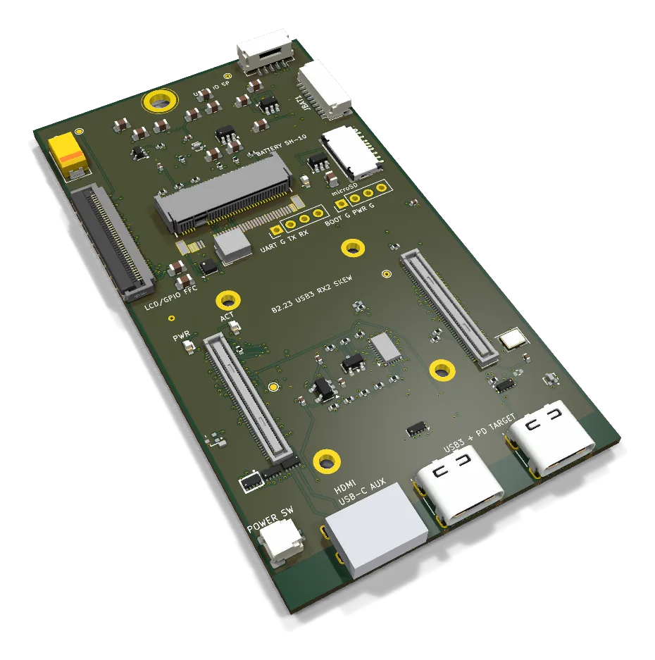
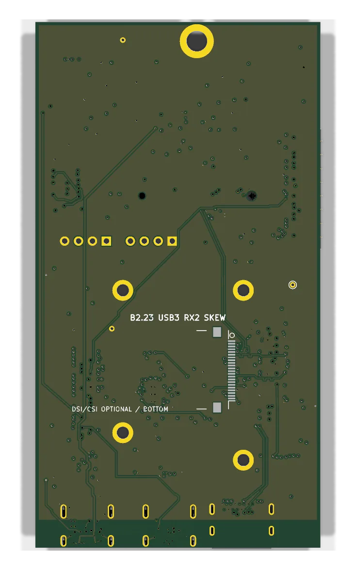
B2.23

USB 3 RX2 skew correction

Withdrawn · mirrored footprints B2 line · compact portrait

Retunes the Type-C RX2 pair after the through-via reroute. Withdrawn: later SMT review exposed mirrored footprints at five parts, so this tree is historical evidence only and must not be fabricated.

Outline
52 × 96 mm
Layers
6 Cu
Footprints
92
Branch
main
Commit
0169447806
B2.23 perspective render
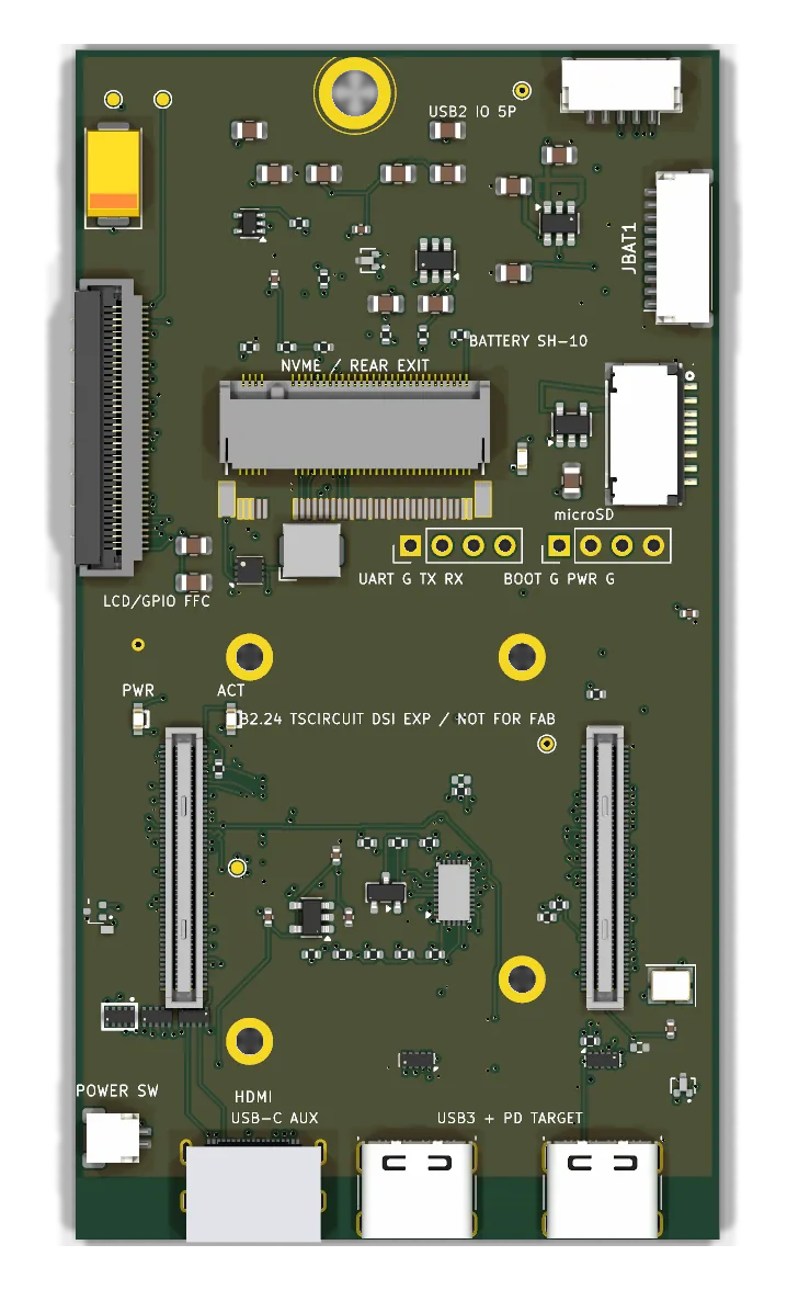
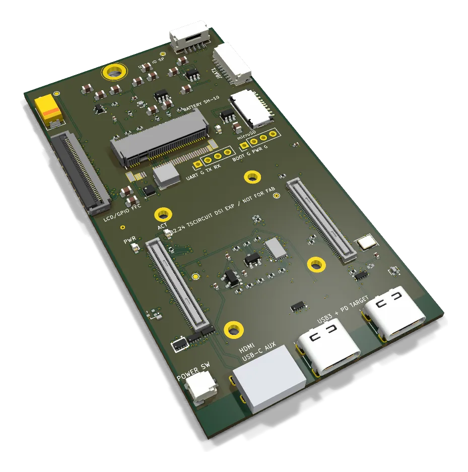
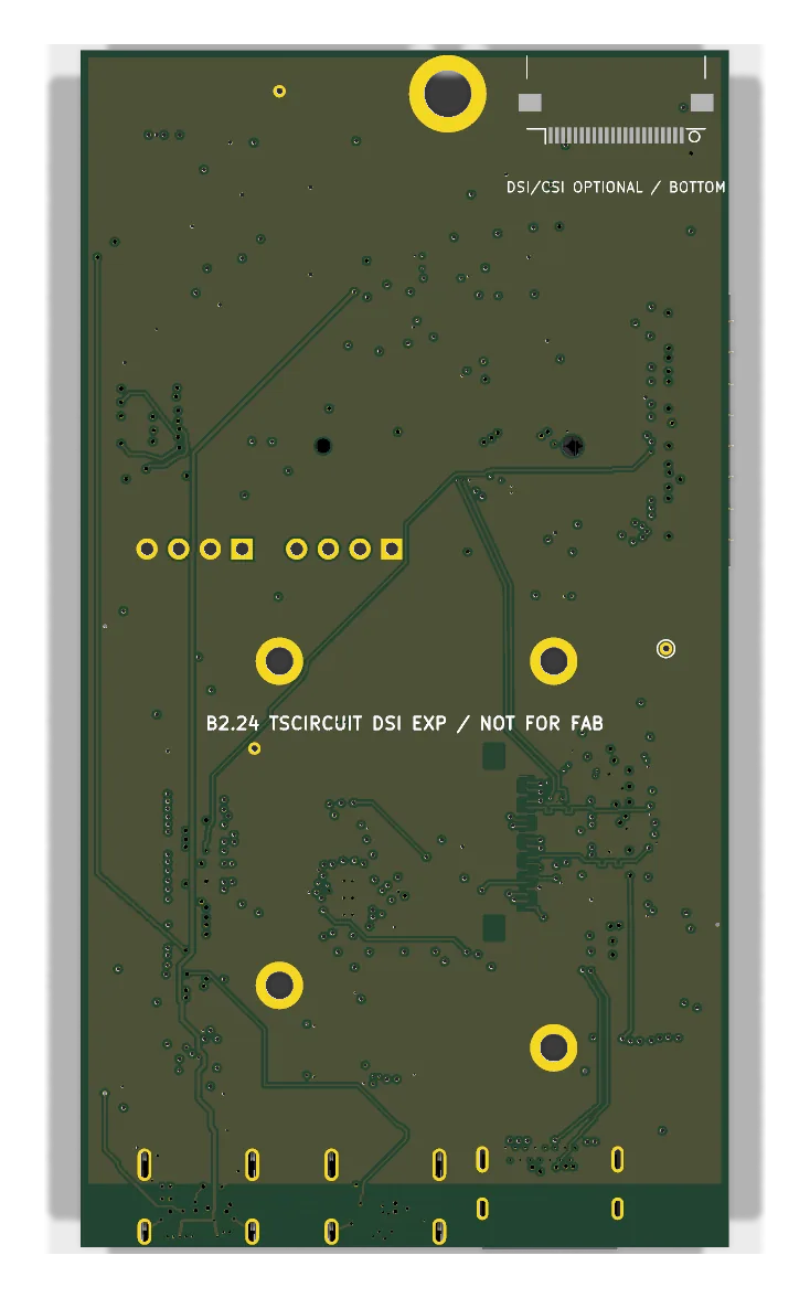
B2.24 (tscircuit)

tscircuit DSI/CSI placement experiment

Routing experiment B2 line · compact portrait experiment

Experimental, immutable fork of B2.23 that evaluates tscircuit's KiCad-to-Circuit-JSON conversion and capacity autorouter on the optional 22-pin DSI/CSI interface.

Outline
52 × 96 mm
Layers
6 Cu
Footprints
92
Branch
codex/b2.24-tscircuit-dsi-experiment
Commit
08fff2cf58
B2.24 (tscircuit) perspective render
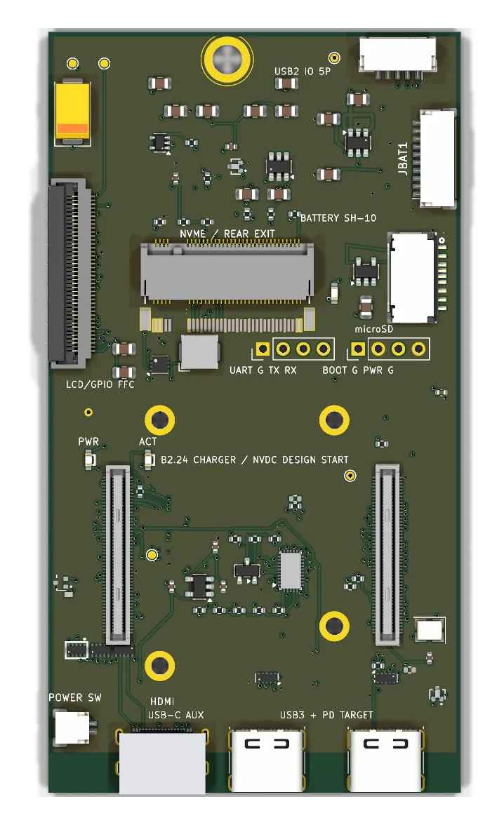
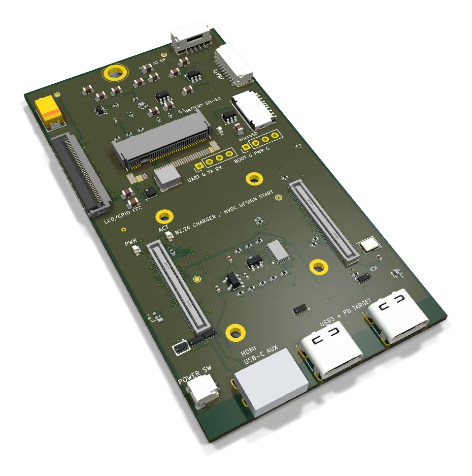
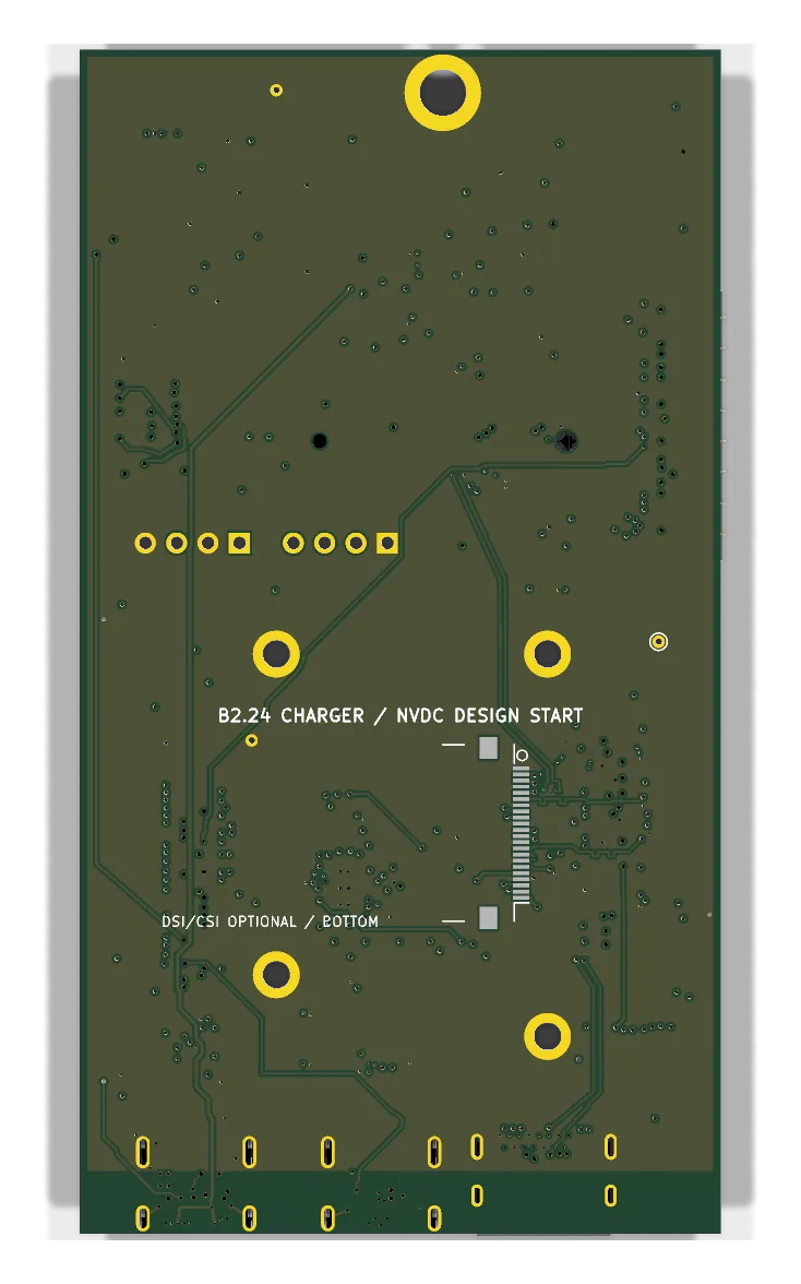
B2.24 (charger)

Charger and NVDC design start

Design start · not fab-ready B2 line · compact portrait

Starts from the released B2.22 source and is reserved for the protected 2S pack charger, NVDC power path and a regulated 5 V system rail. No charger parts are on the board yet; the release command fails closed until the electrical decisions are complete.

Outline
52 × 96 mm
Layers
6 Cu
Footprints
92
Branch
codex/b2.24-charger-nvdc
Commit
026938fc18
B2.24 (charger) perspective render
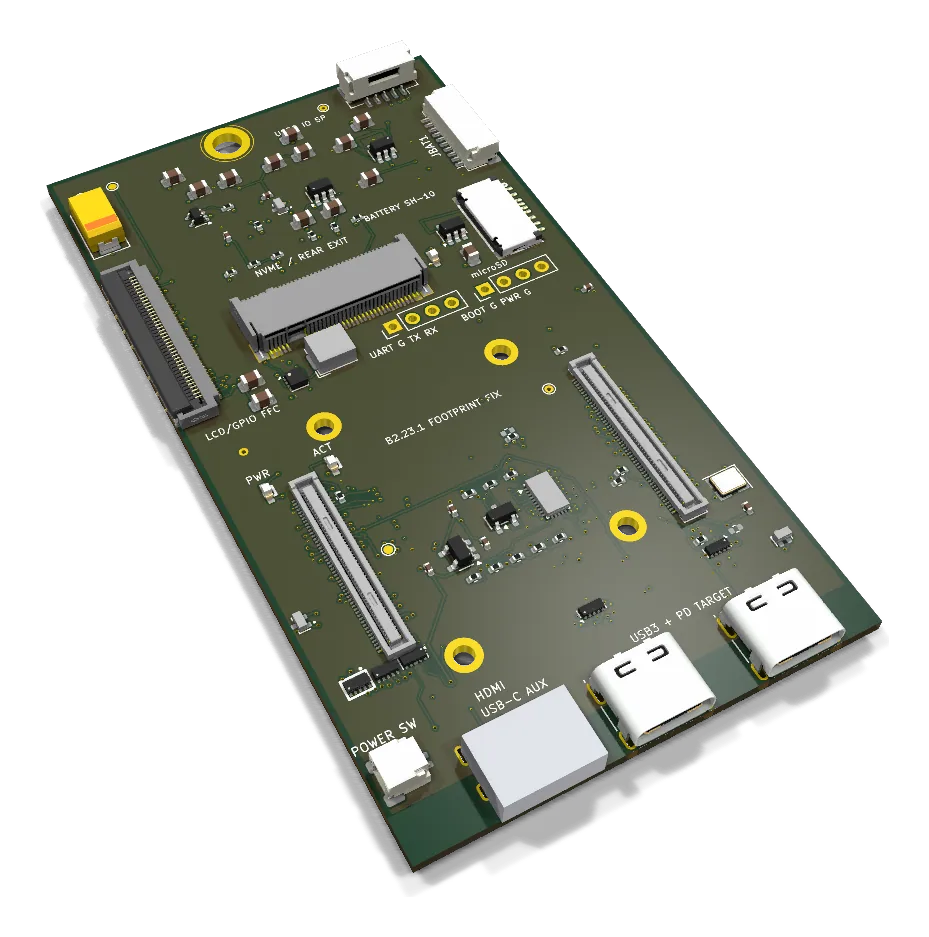
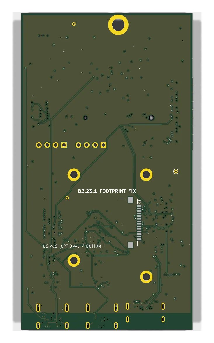
B2.23.1

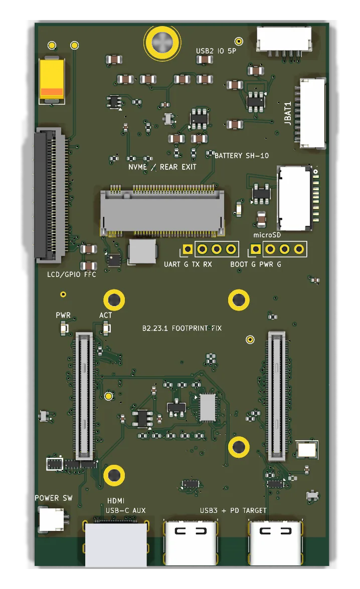
Mirrored-footprint correction

Gates pass · candidate B2 line · compact portrait

Replaces nine reflected generated land patterns with independently library-loaded stock geometry, preserving pad nets and rerouting the affected copper through the official KiCad IPC API. All engineering checkpoint gates pass.

Outline
52 × 96 mm
Layers
6 Cu
Footprints
92
Branch
main
Commit
0169447806
B2.23.1 perspective render
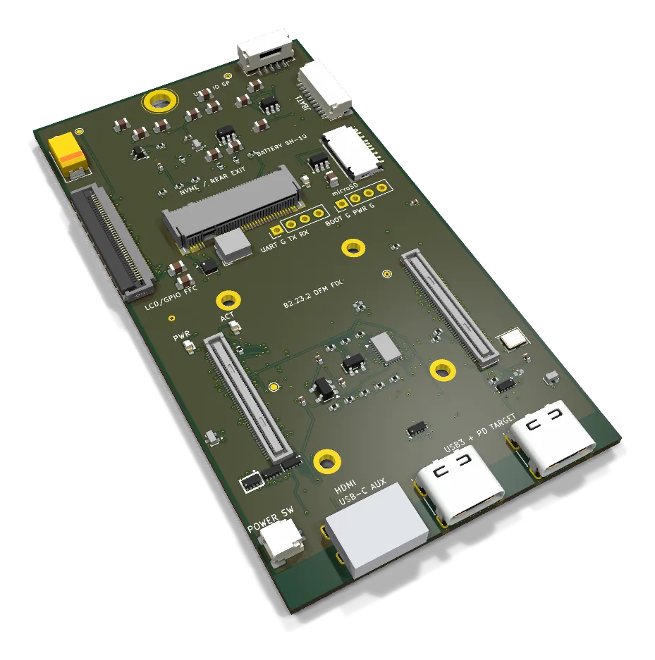
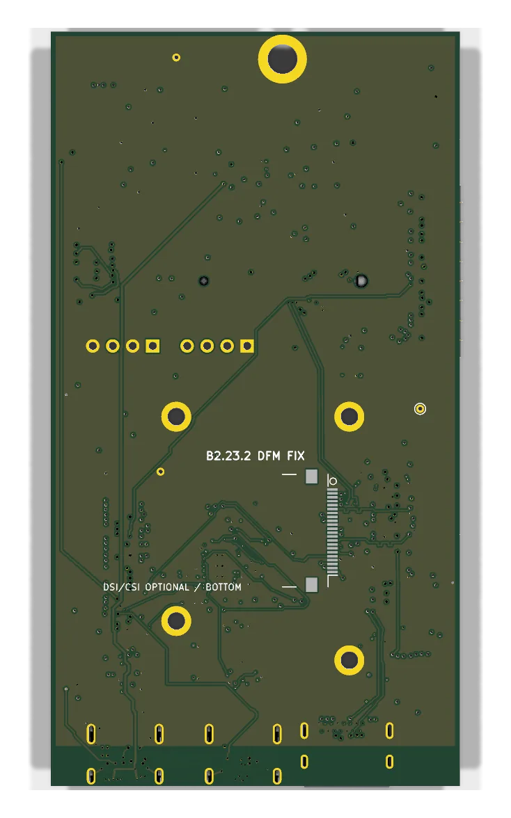
B2.23.2

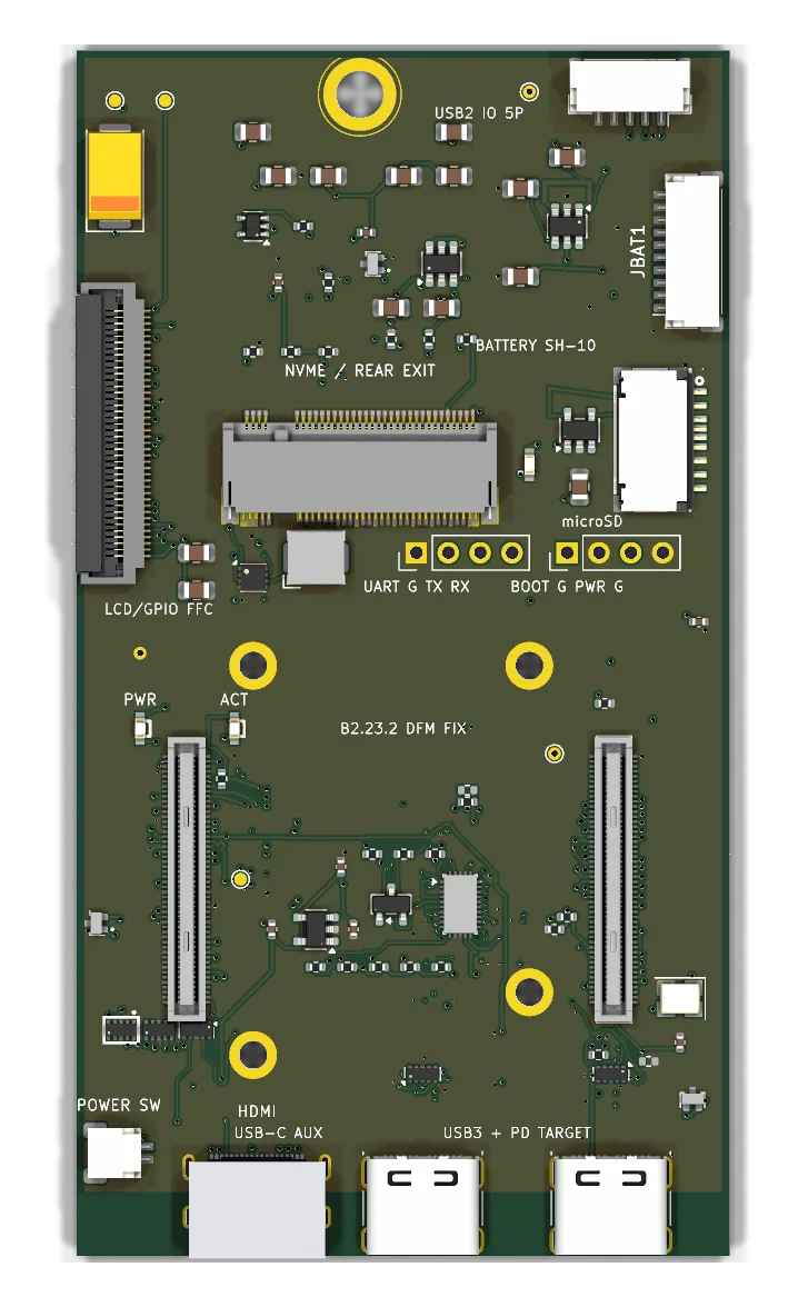
Manufacturing-minima correction

Uploaded for review B2 line · compact portrait

Widens all 50 unsupported 0.07/0.08 mm segments to 0.10 mm with bounded clearance repairs and moves no component. Native DRC: zero errors, zero warnings, zero opens. Uploaded to the assembler's cart for review.

Outline
52 × 96 mm
Layers
6 Cu
Footprints
92
Branch
main
Commit
0169447806
B2.23.2 perspective render
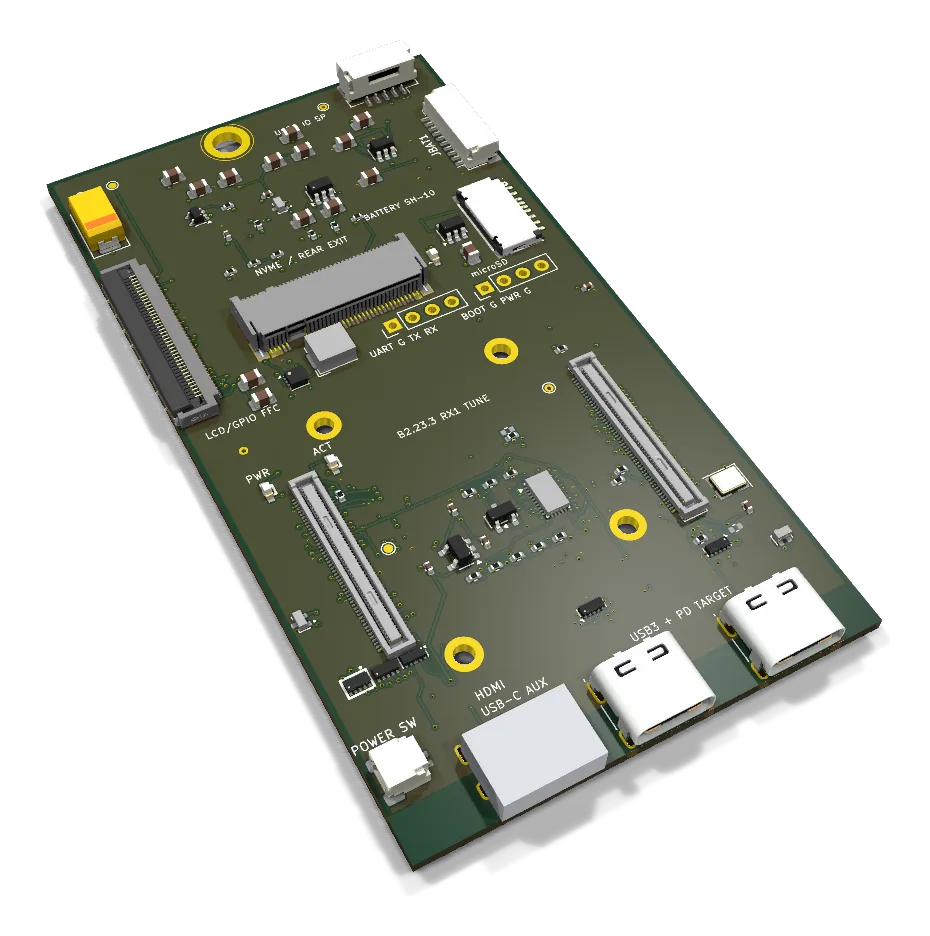
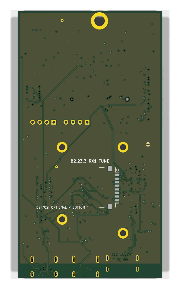
B2.23.3

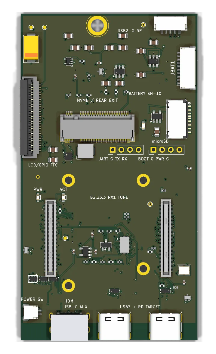
RX1 skew tuning

Head of main B2 line · compact portrait current

Shifts an existing RX1 dogleg by 0.07 mm to bring the pair's endpoint-length proxy from 0.14 mm to about 0.003 mm. Track widths, components and vias unchanged. The current head of main.

Outline
52 × 96 mm
Layers
6 Cu
Footprints
92
Branch
main
Commit
0169447806
B2.23.3 perspective render
B2.24

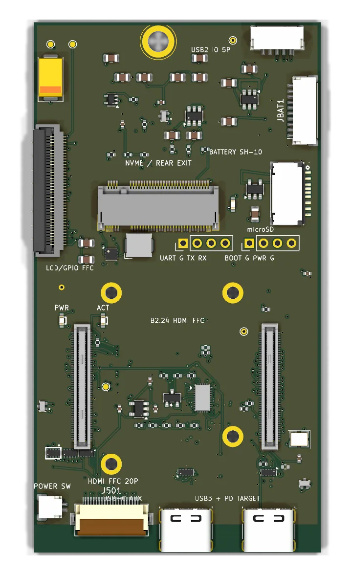
20-pin HDMI FFC fork

Development fork B2 line · compact portrait

Development fork from B2.23.3 that replaces the out-of-stock Mini HDMI receptacle with a stocked Hirose 20-pin 0.5 mm FFC connector using the standard DIY-HDMI pin order and a catalogue cable. Only the HDMI connector and its local fanout may change.

Outline
52 × 96 mm
Layers
6 Cu
Footprints
92
Branch
codex/b2.24-hdmi-ffc
Commit
75f04f34e7
B2.24 perspective render
B2.24.1

Top-side 20-pin HDMI FFC

Fabrication release · latest B2 line · compact portrait latest

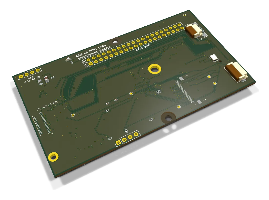
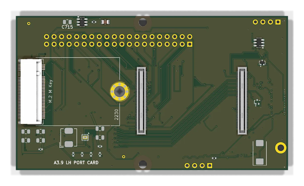
The routed, release-gated version of the HDMI FFC change with the connector on the top side at the bottom edge and every fitted part on the front. Uses the reversed local pin map that an opposite-contact cable requires, locked in a machine-readable connector contract.

Outline
52 × 96 mm
Layers
6 Cu
Footprints
92
Branch
codex/b2.24-hdmi-ffc
Commit
75f04f34e7
B2.24.1 perspective render

Renders and models generated Sep 2, 2026 with KiCad from the revision sources; assets stored in the site repository.