Why the VAIO P
Sony sold the VAIO P from 2009 as a "lifestyle PC": a clamshell the size of a business envelope with a full-width keyboard, a TrackPoint-style stick and an 8-inch 1600 × 768 display. Inside it ran an Intel Atom Z5xx on a Poulsbo chipset that was slow on the day it shipped. The chassis, keyboard and screen have aged far better than the silicon, so we are keeping them and replacing the Foxconn MBX-187 logic board.
The team works from two donors: a VGN-P92KS with a JIS keyboard that is fully stripped, and a VGN-P92LS kept intact as the working reference.
The boards
The CM5 carrier started as a fork of Pierluigi Colangeli's open CM5 MINIMA Rev 2, the smallest routed and manufactured CM5 carrier with same-edge USB-C and onboard M.2 2230. It has since been through 68 revisions in three shapes — 78 × 52 mm, a slim 91.69 × 52 mm landscape board, then a 52 × 96 mm portrait board — and every one of them is on the revision history page with renders and a 3D model.
| Board | What it does |
|---|---|
| CM5 carrier | Compute Module 5 on 1.5 mm Amphenol sockets, M.2 2230 NVMe, USB-C power and a USB 3 host port (TI HD3SS3220), microSD, HDMI over FFC, a 40-pin link to the I/O side |
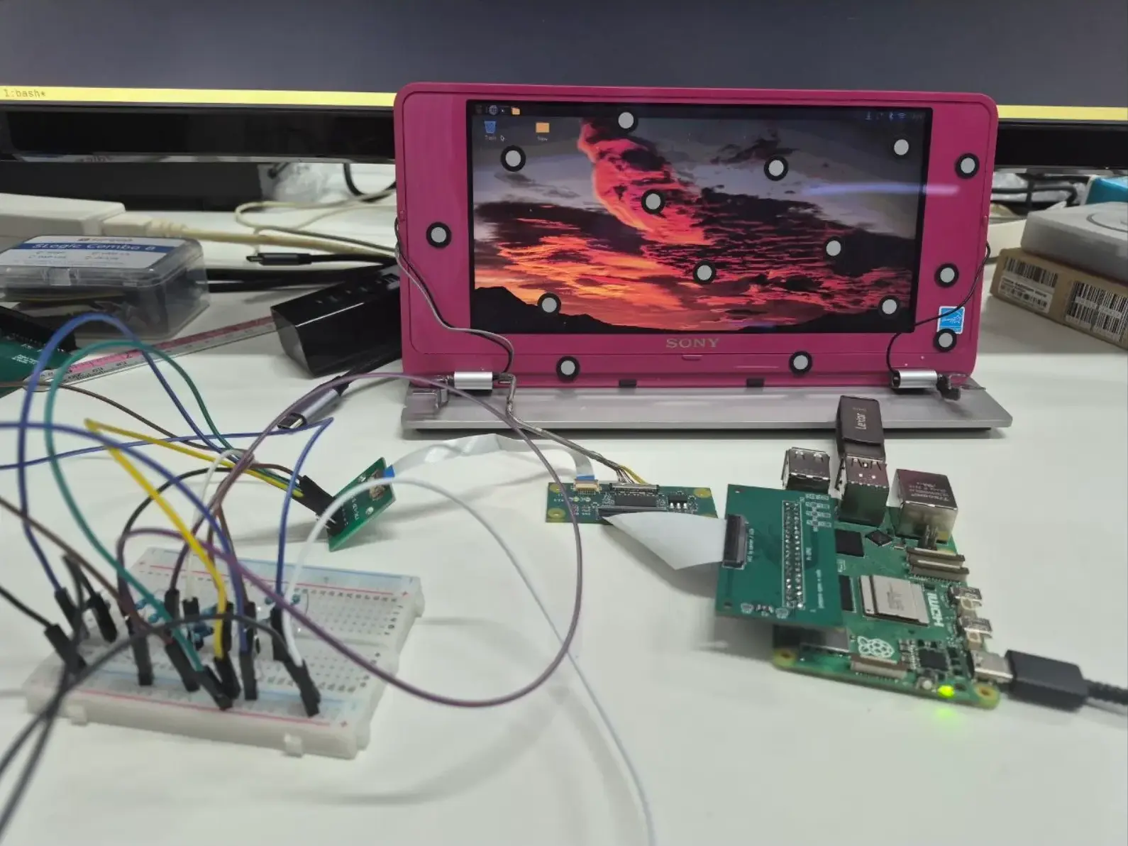
| Koyomi LVDS | Pi DPI (RGB666) → TI SN75LVDS83B → the panel's non-standard 30-pin LVDS at 2.5 V logic, 83.6 MHz, 59.9 Hz |
| Keyboard adapter | RP2040 running QMK: the 8 × 16 matrix and PS/2 pointing stick, presented to the CM5 as USB HID |
| Side I/O | FE1.1s USB 2.0 hub feeding the side ports and the keyboard |
| Battery board | B8.3, a 2 A path to the original 2S pack over a JST SH-10 link |
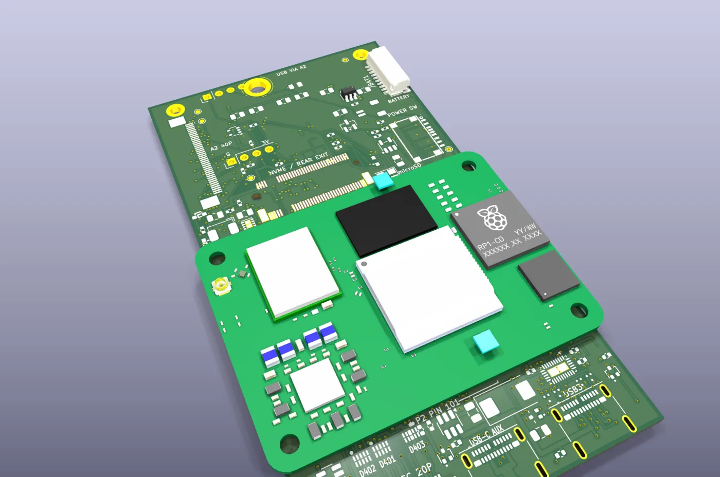
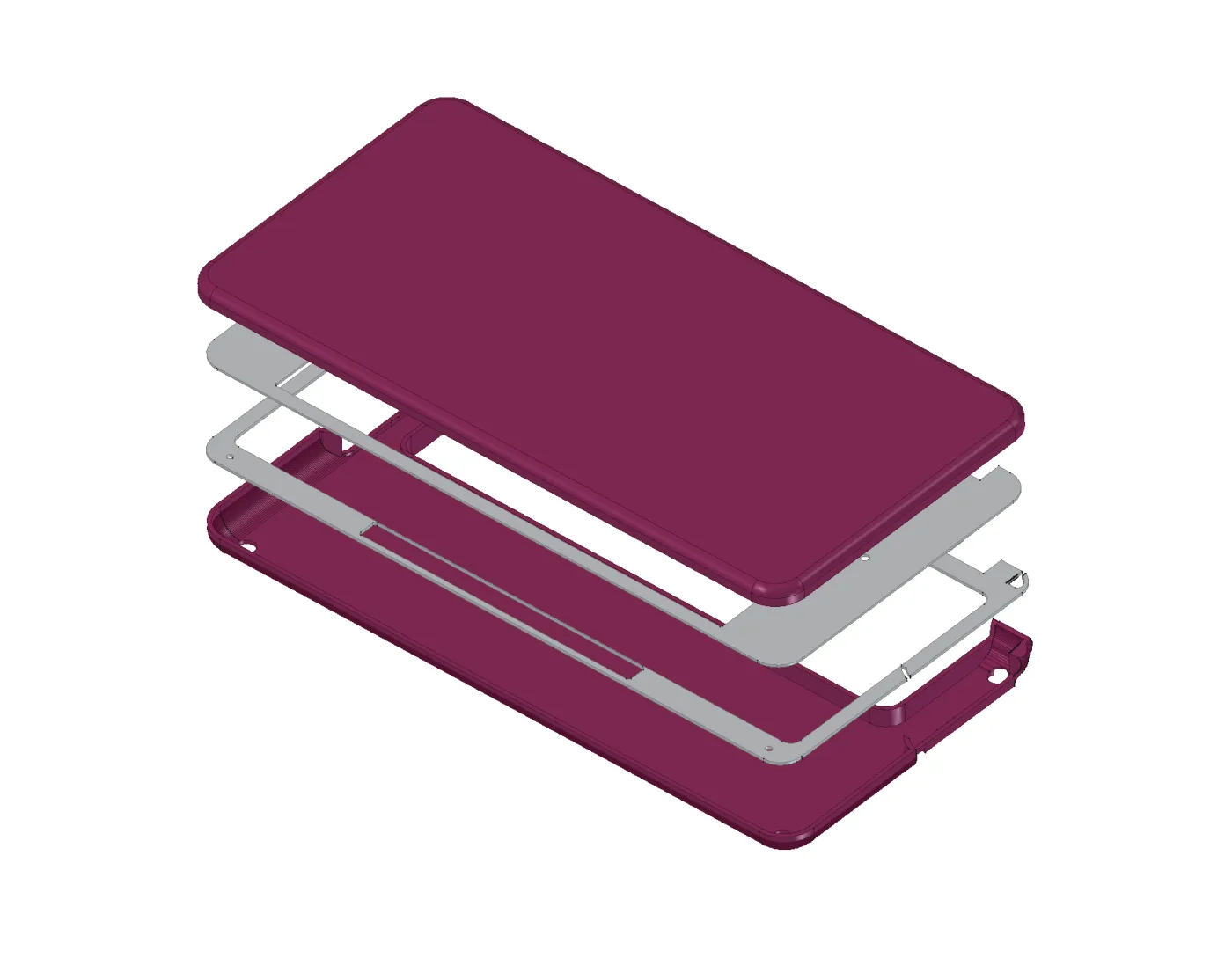
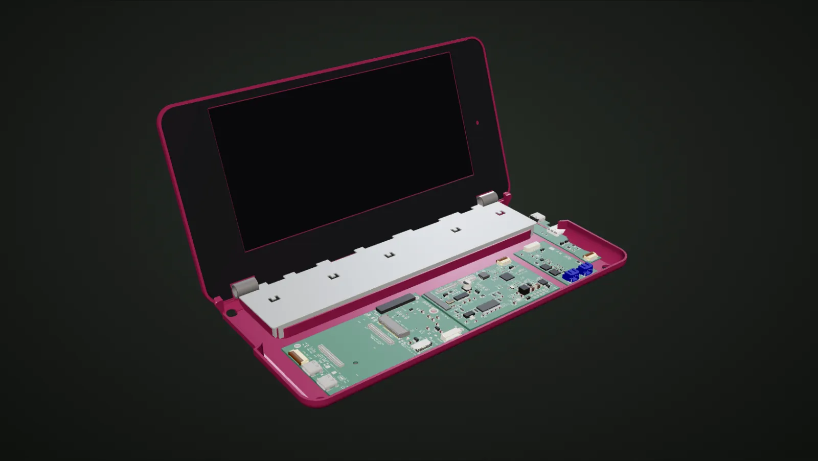
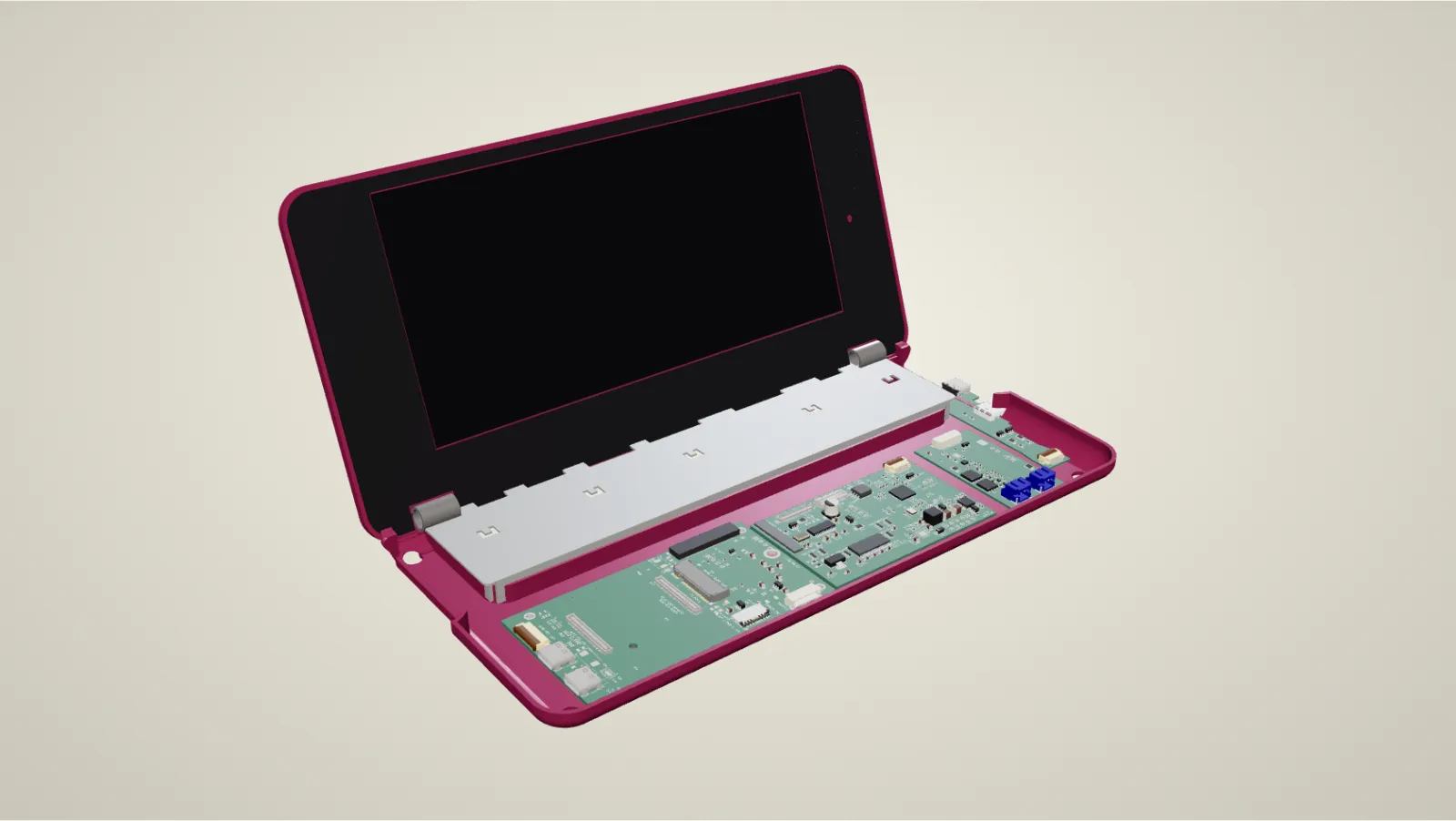
The current layout folds the display bridge, backlight driver and keyboard controller into one combined board, A2, joined to the carrier by a single 40-pin cable. The 3D view above shows that arrangement: carrier B2.28, A2, the battery board and the right-hand port board, placed as in our shell explorer.
Every link between boards has to be an off-the-shelf catalogue cable with one-to-one pin order. A release script checks each connector against a written interconnect contract before anything is ordered.
What made it hard
Height, not area
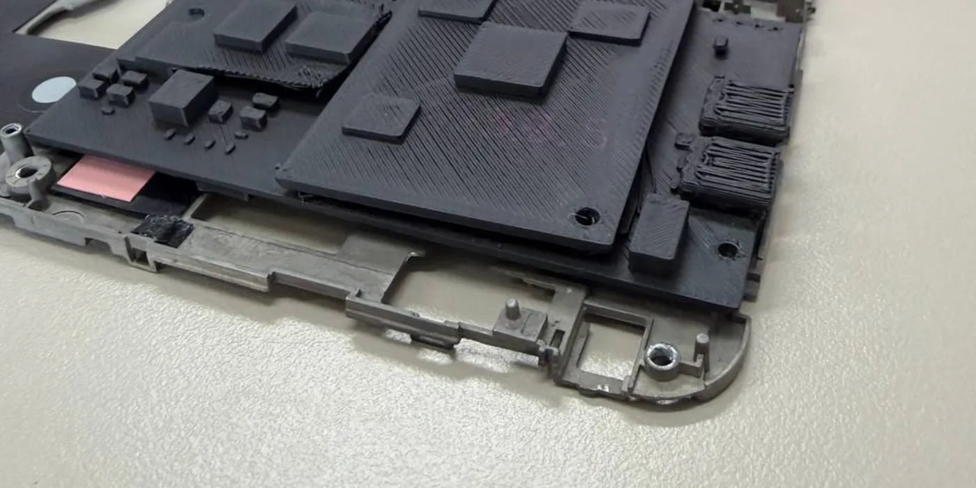
The whole machine is 19.8 mm thick. A CM5 stands 4.94 mm above its carrier even on the lowest socket, and 3D scans put the usable cavity at about 7.1 mm. Early plans put the module in the 1.8" drive bay; at 6.3 mm deep it could never have fit, so the carrier moved to the mainboard cavity at the front left of the base.
The mirrored socket pair
Every B-series carrier from B2.11 to B2.27 placed the two 100-pin CM5 sockets as a mirror image of the module. It mated mechanically, but pin n of the module landed on pad n ± 100. A photo of a CM5 seated on a delivered board exposed it on 21 September. B2.28 turns the module to landscape and adds a fail-closed handedness check to the release gates.
Trusting the wrong 3D model
From B2.17 the USB-C receptacles sat backwards in copper, mouths facing into the board. A home-made 3D model rendered them facing outward and hid it. Orientation is now only checked against vendor drawings and official STEP files.
Heat and sleep
The VAIO P has no fan and was built around a ~2 W-class Atom. We cap sustained power at about 4.5 W for the SoC and 7 W for the system, and spread heat through a nickel-plated plate and flattened heat pipe. The CM5 cannot suspend today, so closing the lid turns the screen off with the machine still drawing 2.4–3.3 W.
Software
The desktop we are aiming for is Omarchy on the CM5 — our aarch64 build of Omarchy's Hyprland desktop, which already boots to a full desktop on a CM5 IO board. The VAIO panel's display overlay is the piece still to be wired into that image.
Build log from X
The carrier and its companion boards, as posted along the way by @kanwisher.
-
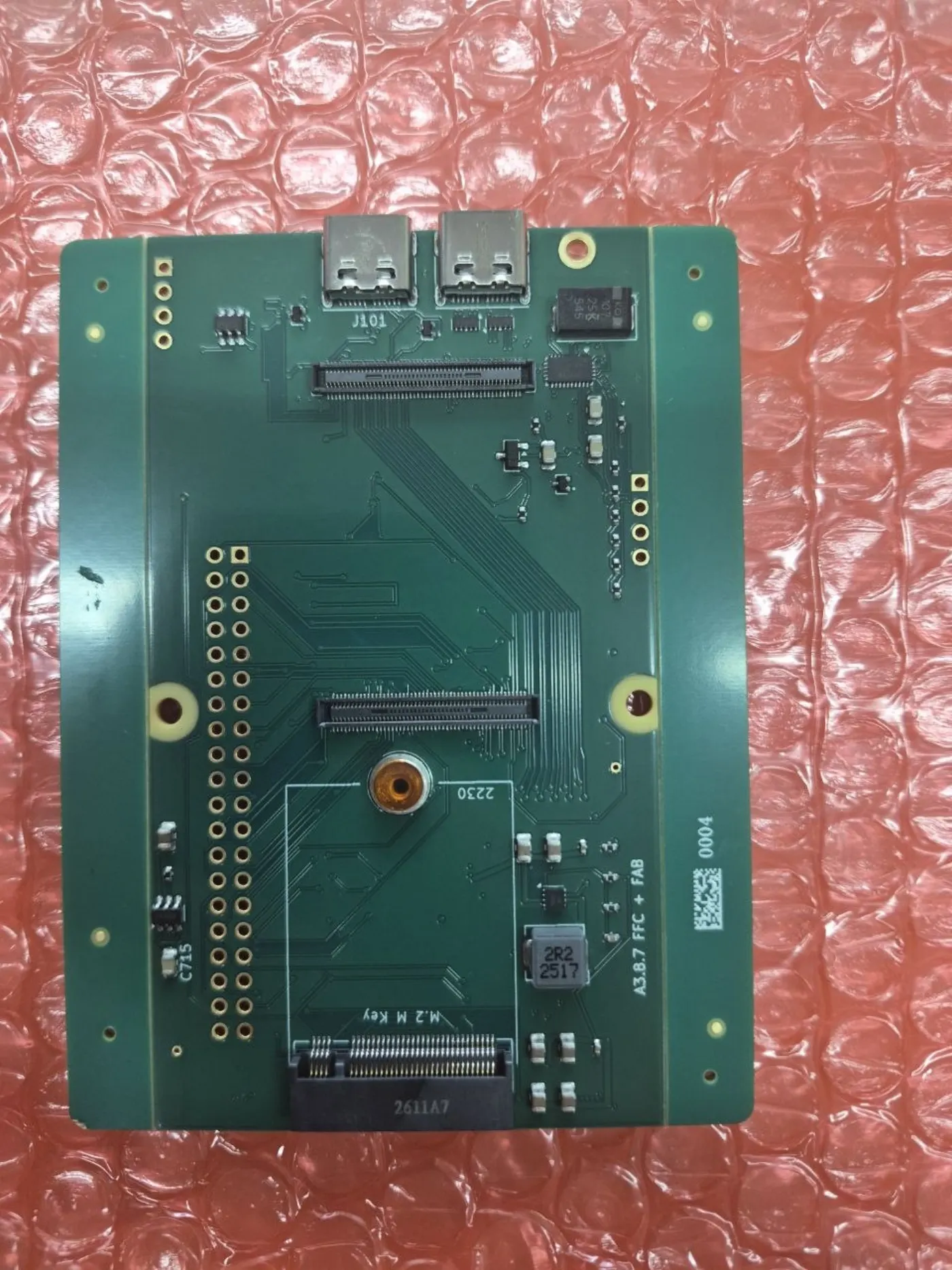
I just got my vibe coded cm5 carrier boards
@kanwisher on X → -
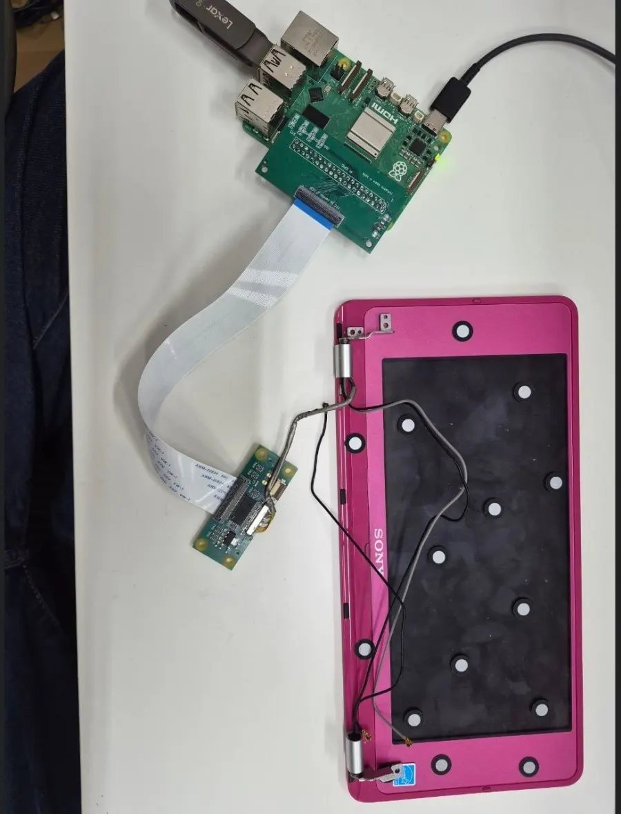
almost have the monitors booted with our custom lcd boards for the Sony Vaio P
 @kanwisher on X →
 -
LCD board is nearly ready, connected to the Sony vaio p monitor
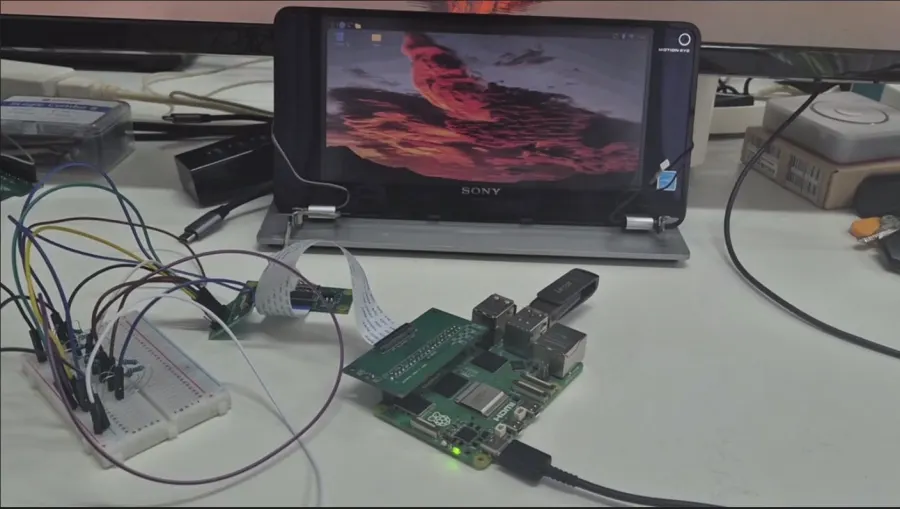 @kanwisher on X →
 -
Gpt6-Astra just built 3d models of exploded view of this Sony Vaio P and the 6 new circuit boards we built so we can visualize our hacking project
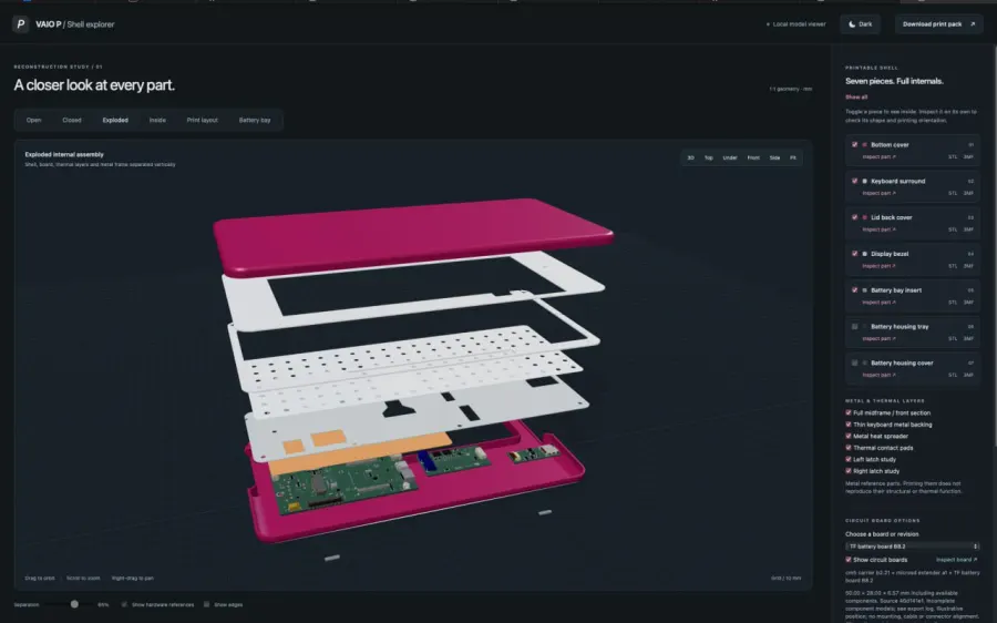 @kanwisher on X →
 -
Keyboard pcb for the Sony vaio looking good . We are getting close to finishing up the Vaio P project
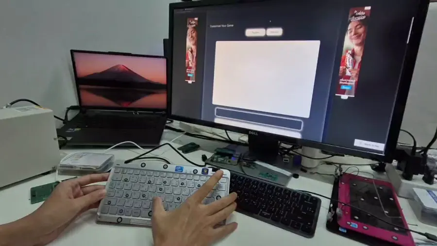 ▶ Video @kanwisher on X →
 -
Theee more Sony Vaio P have come ready to mod, the previous owner ran x86 raspberry pi os lol
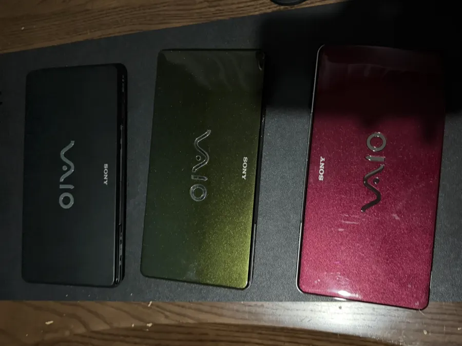 @kanwisher on X →
 -
New board came today, Vaio P replacement is getting close
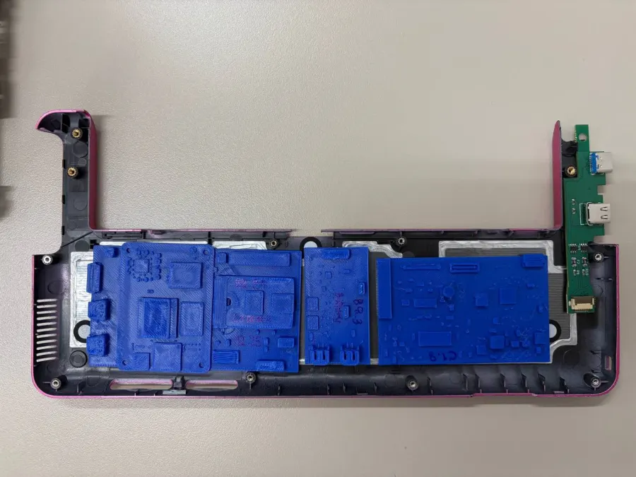 @kanwisher on X →
 -
New carrier boards came for my Sony Vaio P project. Completely vibe coded in Codex , almost there maybe one more rev and I’ll be finished
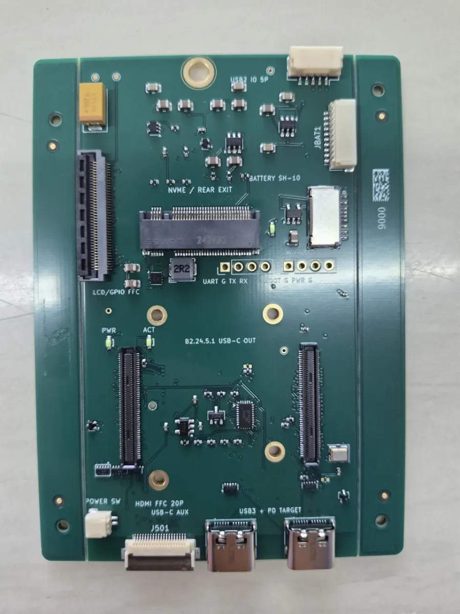 @kanwisher on X →
 -
Vaio P laptop replacement now has a Pi Cm 5 mainboard, custom led board, custom usb boards, hooked up and powered . Now we just need to finish battery boards and reverse engineer Sony battery protocols
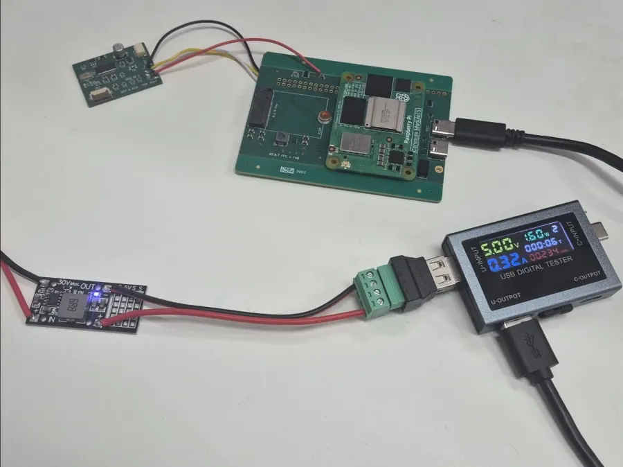 ▶ Video @kanwisher on X →
Status. A carrier has booted a CM5, the original panel has shown a desktop, and the keyboard and pointing stick work through QMK. B2.28 is in fabrication. Still open: battery charging and USB-PD, measuring the mainboard cavity, a backlight driver, and closing it all up inside the chassis.