

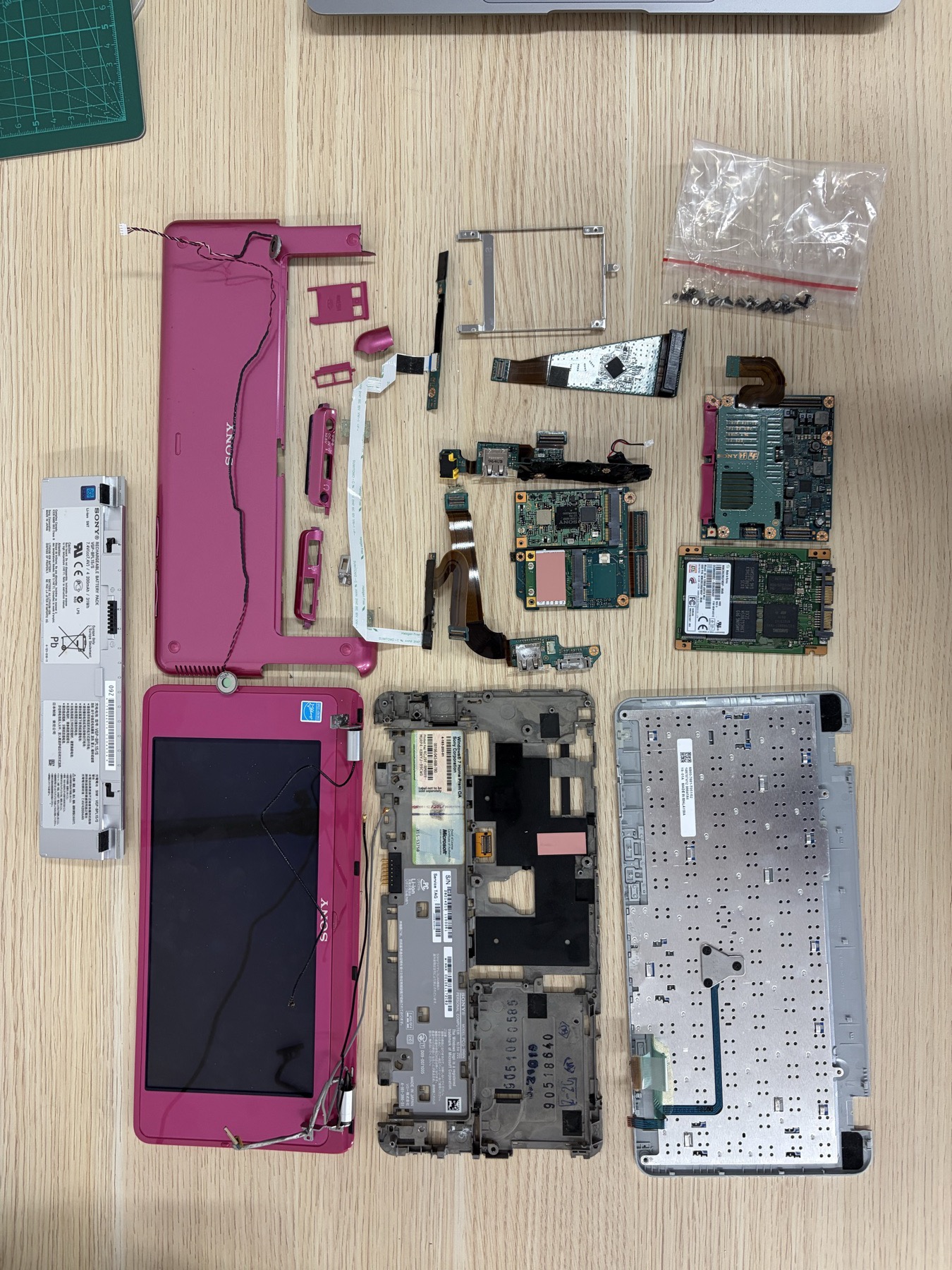
This is where the VAIO P project stopped being an idea and became a packaging problem. We opened the donor, laid out every part, measured the useful spaces, and started turning those measurements into replacement board shapes.
Start with the VAIO P CM5 overview for the project hub.
Donor machine
Our donor is a Japanese-market VAIO P that still boots Windows 7. It is in good condition, which made the teardown feel a little more serious. The shell, keyboard, display, battery bay, and side openings all need to survive the experiment.
The old computer is expendable. The body is the reason for doing this at all.
Teardown approach
The first rule of this teardown was simple: do not pull until we know what is still attached. Flat-flex cables disappear under boards, fold around posts, and reappear at the side I/O and storage assemblies. A part can look loose while a delicate cable is still doing all the holding.
The side I/O was the most useful discovery. Sony did not force the power jack, USB ports, and headphone jack onto one large motherboard. It used small boards that fold and stack into the edges of the shell. Our replacement is likely to follow that pattern rather than pretending one large rectangle will fit.
Measurements
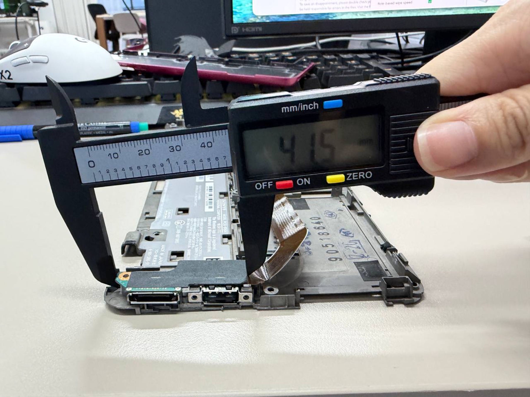
These are our first-pass dimensions from calipers, reference photos, and 3D scans. They are design constraints, not final fabrication numbers.
| Part or bay | Measurement | Why it matters |
|---|---|---|
| Main chassis bay | 133.4 mm | Total horizontal room available for the replacement mainboard area. |
| Original motherboard envelope | 65.4 x 74.8 x 6.9 mm | Reference volume for the original compute electronics. |
| Outer shell envelope | 244.37 x 123.94 x 13.96 mm | Overall bounding box from 3D scans. |
| Side-I/O assembly | 99.0 mm span | Space used by the original peripheral-port strip. |
| Port pocket | 41.5 mm span | Bracket area available for the USB stack and power input. |
Carrier-board plan
We are designing around a Raspberry Pi CM5 Wireless 4GB Lite. Because this module has no eMMC, boot storage has to live elsewhere. An SD slot on an I/O board is the simple option. NVMe on the carrier is faster but takes more room.
The current layout breaks the computer into six boards:
- carrier board
- I/O board
- LCD board
- right-hand side board
- left-hand side board
- battery board
The left and right boards replace Sony’s original side modules. This lets us add modern ports such as USB-C while keeping them aligned with the factory openings.
Printed fit checks
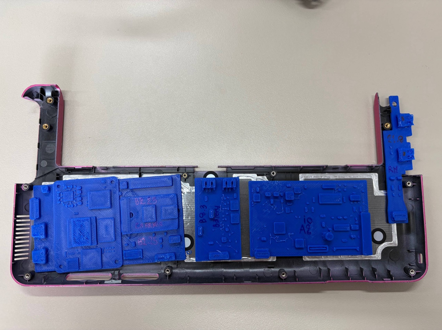
Before ordering real PCBs, we printed the board outlines at 1:1 scale. The mockups are cheap, quick to revise, and surprisingly good at exposing bad connector positions. A3.8.5, Rev H, and A10 are snapshots along that fit-check path, not polished release names.
That is the lesson from this stage: PCB design here is mechanical design. The circuit can be electrically perfect and still fail if a cable cannot bend or the shell will not close.