

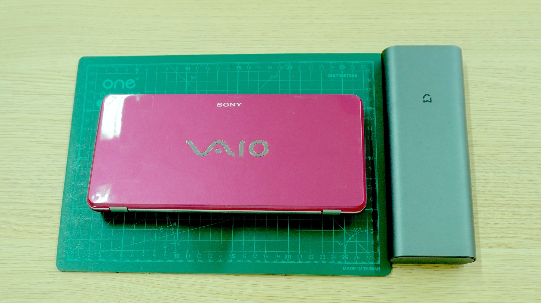
The Sony VAIO P is the sort of computer that still makes people stop and look. It is barely larger than a business envelope, yet Sony managed to fit an 8-inch 1600 x 768 display, a real keyboard, a pointing stick, speakers, and a removable battery into it.
The shape aged better than the Atom hardware inside it. Our plan is to keep the parts that still make the VAIO P special and rebuild the computer around a Raspberry Pi Compute Module 5.
What we are building
This is not a generic computer stuffed into a convenient shell. We want the finished machine to open, type, point, and travel like a VAIO P. The original clamshell, LCD, keyboard, pointing stick, speaker layout, battery bay, and pocketable footprint all stay.
Behind those parts, almost everything changes: motherboard, display interface, keyboard controller, power, storage, side I/O, and internal board layout.
Opening the donor made the real challenge obvious. There is no generous empty rectangle waiting for a new motherboard. Sony used stacked boards, folded flex cables, and narrow side modules to occupy nearly every pocket of the chassis. The CM5 version will need the same kind of spatial thinking.
The project, one problem at a time
We started by photographing and disassembling the donor, then measuring the spaces left by Sony’s motherboard and side boards. Those measurements are feeding printed 1:1 board mockups before we spend money on fabricated PCBs.
The display is a project by itself. The original panel uses LVDS, which the Raspberry Pi does not output directly. Project Koyomi gives us a practical route from Raspberry Pi DPI to the Sony panel, including the unusual 2.5 V panel logic and the original cable’s pin remapping.
The keyboard needs its own adapter too. Its 50-pin, 0.4 mm pitch connector is not something we can probe casually with jumper wires, so the first step is a breakout board. Once the matrix is mapped, an RP2040 can turn the original keyboard into a normal USB HID device.
Then the CM5 carrier has to fit around everything else: boot media, power, display wiring, keyboard USB, antennas, cooling, and replacement side ports. In a machine this thin, connector height and cable bends matter just as much as the PCB outline.
Early measurements
| Part or bay | Measurement | Why it matters |
|---|---|---|
| Main chassis bay | 133.4 mm | Total horizontal room available for the replacement mainboard area. |
| Original motherboard envelope | 65.4 x 74.8 x 6.9 mm | Reference volume for the original compute electronics. |
| Outer shell envelope | 244.37 x 123.94 x 13.96 mm | Overall bounding box from 3D scans. |
| Side-I/O assembly | 99.0 mm span | Space used by the original peripheral-port strip. |
| Port pocket | 41.5 mm span | Bracket area available for the USB stack and power input. |
VAIO P modding series
This page is the front door to the project. Each part of the rebuild has its own working article, so we can update one problem without turning the overview into a wall of notes:
- Core CM5 modding guide: teardown order, parts layout, measurements, board envelopes, carrier-board planning, and integration order.
- VAIO P LCD board guide: LVDS pin mapping, Project Koyomi, 2.5 V panel power, backlight control, and first-light testing.
- VAIO P keyboard-to-USB guide: AXK750147G breakout, matrix scanning, pointing-stick support, and USB HID firmware.
- Windows 7 setup guide: driver notes, recovery media, and baseline behavior before teardown.
- Linux setup guide: display overlay, keyboard firmware, brightness, battery reporting, and power management on the rebuilt machine.
- Open-source VAIO P mod comparison: Project Koyomi, CRImier’s replacement mainboard work, and Omniwing’s completed rebuild.
Building in the open
We are not starting from zero. Project Koyomi is the strongest reference for the display path. CRImier’s reverse-engineering work is useful when thinking about a replacement motherboard, and Omniwing’s completed rebuild shows what happens when all the mechanical compromises finally meet inside a working machine.
That is also why we are separating this into several articles. A working VAIO P conversion will not come from one magic PCB. It will come from a series of small, testable wins that other builders can inspect and reproduce.